TIDUBE1D January   2016  – August 2024


  1.   1
  2.   Description
  3.   Resources
  4.   Features
  5.   Applications
  6.   6
  7. 1System Description
    1. 1.1 Key System Specifications
  8. 2System Overview
    1. 2.1 Block Diagram
    2. 2.2 Highlighted Products and Key Advantages
      1. 2.2.1 UCC28180 – PFC Controller
      2. 2.2.2 UCC27524 – Dual Low-Side Gate Driver
      3. 2.2.3 UCC28881 – 700-V Off-Line Converter
    3. 2.3 System Design Theory
      1. 2.3.1 Selecting Switching Frequency
      2. 2.3.2 Calculating Output Capacitance
      3. 2.3.3 Calculating PFC Choke Inductor
      4. 2.3.4 Selecting Switching Element
      5. 2.3.5 Boost Follower Control Circuit
      6. 2.3.6 Bias Power
      7. 2.3.7 On-Off Switch
      8. 2.3.8 Thermal Design
  9. 3Hardware, Testing Requirements, and Test Results
    1. 3.1 Required Hardware
      1. 3.1.1 Test Conditions
      2. 3.1.2 Recommended Equipment
      3. 3.1.3 Procedure
    2. 3.2 Test Results
      1. 3.2.1 Performance Data
        1. 3.2.1.1 Efficiency and iTHD
        2. 3.2.1.2 Standby Power and Output Voltage
      2. 3.2.2 Performance Curves
        1. 3.2.2.1 Efficiency Curve
        2. 3.2.2.2 Voltage Follower Performance
      3. 3.2.3 Functional Waveforms
        1. 3.2.3.1 Power On Sequence
        2. 3.2.3.2 Inrush Current Protection
        3. 3.2.3.3 Switching Node
        4. 3.2.3.4 Waveform Under 3.5kW, 230VAC
      4. 3.2.4 Thermal Measurements
  10. 4Design Files
    1. 4.1 Schematics
    2. 4.2 Bill of Materials
  11. 5Documentation Support
  12. 6Trademarks
  13. 7About the Author
  14. 8Revision History

Inrush Current Protection

Figure 3-5 shows inrush current protection feature, board is powered on with switch-on status. Inrush current protection delay time is about 850mS under 220VAC.

Channel 1 is DC output voltage

Channel 2 is AC input voltage

Channel 3 is 15V.

Channel 4 is AC input current
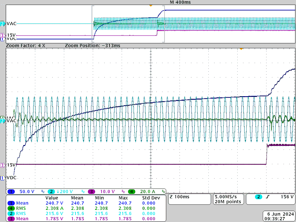
TIDA-00779 Startup and Power On DelayFigure 3-5 Startup and Power On Delay