TIDUBE1D January   2016  – August 2024


  1.   1
  2.   Description
  3.   Resources
  4.   Features
  5.   Applications
  6.   6
  7. 1System Description
    1. 1.1 Key System Specifications
  8. 2System Overview
    1. 2.1 Block Diagram
    2. 2.2 Highlighted Products and Key Advantages
      1. 2.2.1 UCC28180 – PFC Controller
      2. 2.2.2 UCC27524 – Dual Low-Side Gate Driver
      3. 2.2.3 UCC28881 – 700-V Off-Line Converter
    3. 2.3 System Design Theory
      1. 2.3.1 Selecting Switching Frequency
      2. 2.3.2 Calculating Output Capacitance
      3. 2.3.3 Calculating PFC Choke Inductor
      4. 2.3.4 Selecting Switching Element
      5. 2.3.5 Boost Follower Control Circuit
      6. 2.3.6 Bias Power
      7. 2.3.7 On-Off Switch
      8. 2.3.8 Thermal Design
  9. 3Hardware, Testing Requirements, and Test Results
    1. 3.1 Required Hardware
      1. 3.1.1 Test Conditions
      2. 3.1.2 Recommended Equipment
      3. 3.1.3 Procedure
    2. 3.2 Test Results
      1. 3.2.1 Performance Data
        1. 3.2.1.1 Efficiency and iTHD
        2. 3.2.1.2 Standby Power and Output Voltage
      2. 3.2.2 Performance Curves
        1. 3.2.2.1 Efficiency Curve
        2. 3.2.2.2 Voltage Follower Performance
      3. 3.2.3 Functional Waveforms
        1. 3.2.3.1 Power On Sequence
        2. 3.2.3.2 Inrush Current Protection
        3. 3.2.3.3 Switching Node
        4. 3.2.3.4 Waveform Under 3.5kW, 230VAC
      4. 3.2.4 Thermal Measurements
  10. 4Design Files
    1. 4.1 Schematics
    2. 4.2 Bill of Materials
  11. 5Documentation Support
  12. 6Trademarks
  13. 7About the Author
  14. 8Revision History

Switching Node

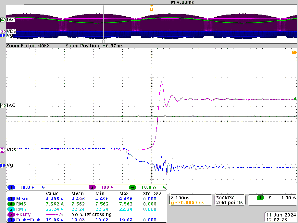
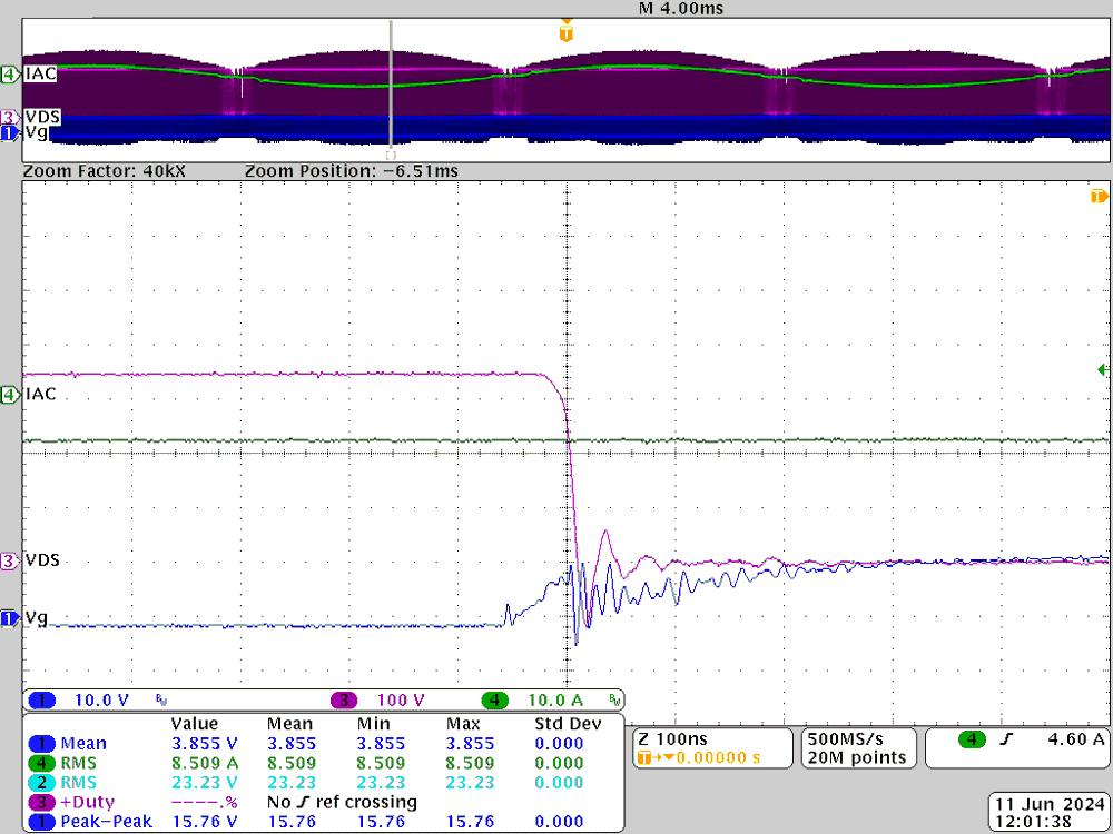
Figure 3-6 and Figure 3-7 show the waveforms at the switching node, which were observed along with the MOSFET for 230V AC.

Channel 1 is Voltage of MOSFET Gate

Channel 2 is AC input voltage

Channel 3 is Voltage of MOSFET Drain to Source

Channel 4 is AC input current
TIDA-00779 Turn on MOSFETFigure 3-6 Turn on MOSFET
TIDA-00779 Turn off MOSFETFigure 3-7 Turn off MOSFET