TIDUBE1D January 2016 – August 2024
- 1
- Description
- Resources
- Features
- Applications
- 6
- 1System Description
- 2System Overview
- 3Hardware, Testing Requirements, and Test Results
- 4Design Files
- 5Documentation Support
- 6Trademarks
- 7About the Author
- 8Revision History
2.3.2 Calculating Output Capacitance
Assuming that the percentage of non-conducting period is minimal, the required output capacitance can be calculated as Equation 3 shows:
Equation 3. 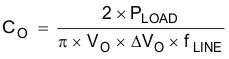
Where
- ΔVO = The peak-to-peak voltage ripple on the output
- fLINE = The input line frequency
- PLOAD = The output load power
Insert the values into Equation 3 to obtain the following result:
Equation 4. 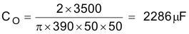
A capacitance of 2040 µF has been selected to accommodate overload conditions and effects caused by aging.