TIDUBF0 January 2022
- Description
- Resources
- Features
- Applications
- 5
- 1System Description
- 2System Overview
- 3Hardware, Testing Requirements, and Test Results
- 4Design and Documentation Support
- 5Tools and Software
- 6Documentation Support
- 7Support Resources
- 8Trademarks
2.2.2.1 POC Filter
One of the most critical portions of a design that uses POC is the filter circuitry. The goal is twofold:
- Deliver a clean DC supply to the input of the switching regulators.
- Protect the FPD-Link communication channels from noise-coupled backwards from the rest of the system.
The DS90UB933-Q1 and DS90UB954-Q1 SerDes devices used in this system communicate over two carrier frequencies, 1 GHz at full speed ("forward channel") and a lower frequency of 2.5 MHz ("back channel") determined by the deserializer device. The filter must attenuate this rather large band spanning both carriers, hoping to pass only DC.
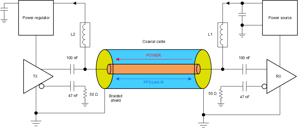
For the POC design, to enable the forward channel and back channel to pass uninterrupted over the coax, an impedance of 1 kΩ across the 1-MHz to 1-GHz bandwidth is required. Use two inductors: a 4.7-µH inductor for high-frequency forward channel filtering, and a 100-µH inductor for low-frequency back-channel filtering. For more details, see the Sending Power Over Coax in DS90UB913A Designs application report. In addition, a 1-kΩ resistor is placed in parallel with both of these inductors. A 1-kΩ ferrite bead is also placed in series for extra filtering at the forward channel data rate.
Lastly, in regards to filtering, ensuring that the FPD-Link signal is uninterrupted is just as important as providing a clean, noise-free DC supply to the system. To achieve this, AC coupling capacitors shown by the 0.1 µF and 0.047 µF are chosen to ensure the high-speed AC data signals are passed through but that the DC is blocked from getting on the data lines.
 Figure 2-4 Power Over Coax