TIDUBF0 January   2022


  1.   Description
  2.   Resources
  3.   Features
  4.   Applications
  5.   5
  6. 1System Description
    1. 1.1 Key System Specifications
  7. 2System Overview
    1. 2.1 Block Diagram
    2. 2.2 Design Considerations
      1. 2.2.1 PCB and Form Factor
      2. 2.2.2 Power Supply Design
        1. 2.2.2.1 POC Filter
        2. 2.2.2.2 Power Supply Considerations
          1. 2.2.2.2.1 Choosing External Components
          2. 2.2.2.2.2 Choosing the Buck 1 Inductor
          3. 2.2.2.2.3 Choosing the Buck 2 and Buck 3 Inductors
        3. 2.2.2.3 Functional Safety
    3. 2.3 Highlighted Products
      1. 2.3.1 OX01F10 Imager
      2. 2.3.2 DS90UB933-Q1
      3. 2.3.3 TPS650320-Q1
    4. 2.4 System Design Theory
  8. 3Hardware, Testing Requirements, and Test Results
    1. 3.1 Hardware Requirements
      1. 3.1.1 Hardware Setup
      2. 3.1.2 FPD-Link III I2C Initialization
      3. 3.1.3 OX01F10 Initialization
    2. 3.2 Test Setup
      1. 3.2.1 Power Supplies Start Up
      2. 3.2.2 Setup for Verifying I2C Communications
    3. 3.3 Test Results
      1. 3.3.1 Power Supplies Start-Up
      2. 3.3.2 Power Supply Start-Up—1.8-V Rail and PDB
      3. 3.3.3 Power Supply Voltage Ripple
      4. 3.3.4 Power Supply Load Currents
      5. 3.3.5 I2C Communications
  9. 4Design and Documentation Support
    1. 4.1 Design Files
      1. 4.1.1 Schematics
      2. 4.1.2 Bill of Materials
      3. 4.1.3 PCB Layout Recommendations
        1. 4.1.3.1 Layout Prints
        2. 4.1.3.2 PMIC Layout Recommendations
        3. 4.1.3.3 Serializer Layout Recommendations
        4. 4.1.3.4 Imager Layout Recommendations
        5. 4.1.3.5 PCB Layer Stackup Recommendations
      4. 4.1.4 Altium Project
      5. 4.1.5 Gerber Files
  10. 5Tools and Software
  11. 6Documentation Support
  12. 7Support Resources
  13. 8Trademarks

I2C Communications

I2C communication between the DS90UB954-Q1 EVM and OX01F10 imager over the FPD-Link III back channel can be confirmed with the Analog LaunchPad GUI. Figure 3-10 and Figure 3-11 show the established link with the serializer on RX port 1, and the corresponding register map.
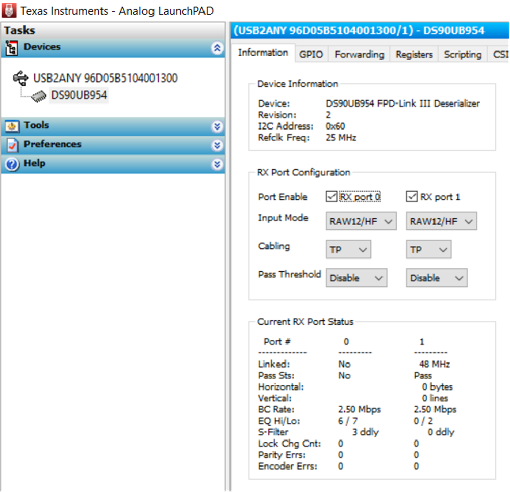
GUID-20211117-SS0I-GRH4-PVDJ-5CPHDMTMSPPK-low.pngFigure 3-10 Analog LaunchPad™ Link Confirmation
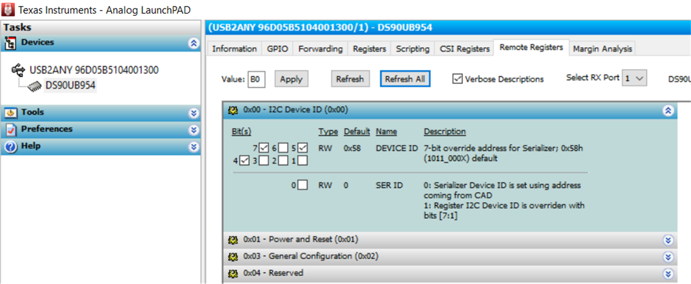
GUID-20211117-SS0I-CZST-0MMT-B90JZHJG7RTS-low.pngFigure 3-11 Serializer Remote Registers

Read and writes to the imager, at slave alias address 0x6C (7-bit), are confirmed with the built-in Python scripting window of the Analog LaunchPad. Register 0x3035 reads data 0x6C, which is the expected default value for the register.
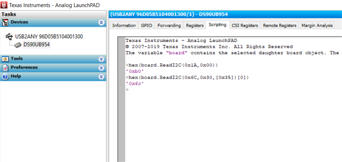
GUID-20211117-SS0I-6ZCQ-SLDG-VZ0HXKCJ1GZW-low.pngFigure 3-12 Back-Channel I2C Communication