TIDUBF0 January 2022
- Description
- Resources
- Features
- Applications
- 5
- 1System Description
- 2System Overview
- 3Hardware, Testing Requirements, and Test Results
- 4Design and Documentation Support
- 5Tools and Software
- 6Documentation Support
- 7Support Resources
- 8Trademarks
2.2.2.2.1 Choosing External Components
For simplicity, the efficiency of the buck regulators is assumed to be 85% for these operating conditions, and the efficiency of the LDO is given by Equation 5.
Table 2-2 shows the load capability of each regulator compared to the requirements of the camera module. The TPS650320-Q1 device is capable of supplying the system power with plenty of margin to account for variations between typical and maximum current variation.
| REGULATOR | OUTPUT VOLTAGE (V) | MAX CURRENT (mA) | REQUIRED CURRENT (mA) |
|---|---|---|---|
| Buck 1 | 3.8 | 800 | 160 |
| Buck 2 | 1.8 | 600 | 122 |
| Buck 3 | 1.1 | 600 | 170 |
| LDO | 3.3 | 300 | 33 |
After determining that the TPS650320-Q1 device is suitable based on the power requirements, the external components can be chosen quickly based on the data sheet recommendations, simplifying the design process. These recommendations are shown in Figure 2-5 and Equation 5.
 Figure 2-5 TPS650320-Q1 Typical Application Circuit
| COMPONENT | DESCRIPTION | VALUE | UNIT |
|---|---|---|---|
| CVSYS,VSYS_S | VSYS and VSYS_S decoupling | 10 | µF |
| CPVIN_B1 | Buck 1 input capacitor | 10 | µF |
| LSW_B1 | Buck 1 inductor | 2.2 | µH |
| COUT_B1 | Buck 1 output capacitor | 10 | µF |
| CPVIN_B2 | Buck 2 input capacitor | 10 | µF |
| LSW_B2 | Buck 2 inductor | 1.0 | µH |
| COUT_B2 | Buck 2 output capacitor | 10 | µF |
| CPVIN_B3 | Buck 3 input capacitor | 10 | µF |
| LSW_B3 | Buck 3 inductor | 1.0 | µH |
| COUT_B3 | Buck 3 output capacitor | 10 | µF |
| CPVIN_LDO | LDO input capacitor | 1.0 | µF |
| COUT_LDO | LDO output capacitor | 2.2 | µF |
The high, fixed PWM 2.3-MHz switching frequency enables the use of small inductors with a fast transient response. A value of 2.2 µH is typically recommended for the BUCK1 channel output. This value helps to minimize the inductor ripple current.
With the inductance value chosen, the design now needs an inductor with a proper saturation current. This is the combination of the steady-state supply current as well as the inductor ripple current. The current rating needs to be sufficiently high but minimized as much as possible to reduce the physical size of the inductor. Calculate inductor ripple with Equation 3:
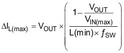
where:
- IL(max) is the maximum inductor current
- ΔIL is the peak-to-peak inductor ripple current
- L(min) is the minimum effective inductor value
- fSW is the actual PWM switching frequency
The parameters for this reference design using the TPS650330-Q1 are:
- VOUT = 3.3 V
- VIN(max) = 18.3 V
- L(min) = 2.2 µH
- fSW = 2.3 MHz
These parameters yield an inductor current of ∆IL = 535 mA. The maximum current draw of the system through this regulator is 327 mA. The minimum saturation current is calculated as:
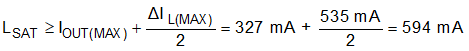
The TPS650330-Q1 device on this design uses a Murata® LQM2MPN2R2NG0, which has a rated current of 1.2 A and a DC resistance maximum of 138 mΩ. Additionally, this device has an operating temperature from –55°C to 125°C and comes in a very small 2-mm × 1.6-mm package.