TIDUBF0 January   2022


  1.   Description
  2.   Resources
  3.   Features
  4.   Applications
  5.   5
  6. 1System Description
    1. 1.1 Key System Specifications
  7. 2System Overview
    1. 2.1 Block Diagram
    2. 2.2 Design Considerations
      1. 2.2.1 PCB and Form Factor
      2. 2.2.2 Power Supply Design
        1. 2.2.2.1 POC Filter
        2. 2.2.2.2 Power Supply Considerations
          1. 2.2.2.2.1 Choosing External Components
          2. 2.2.2.2.2 Choosing the Buck 1 Inductor
          3. 2.2.2.2.3 Choosing the Buck 2 and Buck 3 Inductors
        3. 2.2.2.3 Functional Safety
    3. 2.3 Highlighted Products
      1. 2.3.1 OX01F10 Imager
      2. 2.3.2 DS90UB933-Q1
      3. 2.3.3 TPS650320-Q1
    4. 2.4 System Design Theory
  8. 3Hardware, Testing Requirements, and Test Results
    1. 3.1 Hardware Requirements
      1. 3.1.1 Hardware Setup
      2. 3.1.2 FPD-Link III I2C Initialization
      3. 3.1.3 OX01F10 Initialization
    2. 3.2 Test Setup
      1. 3.2.1 Power Supplies Start Up
      2. 3.2.2 Setup for Verifying I2C Communications
    3. 3.3 Test Results
      1. 3.3.1 Power Supplies Start-Up
      2. 3.3.2 Power Supply Start-Up—1.8-V Rail and PDB
      3. 3.3.3 Power Supply Voltage Ripple
      4. 3.3.4 Power Supply Load Currents
      5. 3.3.5 I2C Communications
  9. 4Design and Documentation Support
    1. 4.1 Design Files
      1. 4.1.1 Schematics
      2. 4.1.2 Bill of Materials
      3. 4.1.3 PCB Layout Recommendations
        1. 4.1.3.1 Layout Prints
        2. 4.1.3.2 PMIC Layout Recommendations
        3. 4.1.3.3 Serializer Layout Recommendations
        4. 4.1.3.4 Imager Layout Recommendations
        5. 4.1.3.5 PCB Layer Stackup Recommendations
      4. 4.1.4 Altium Project
      5. 4.1.5 Gerber Files
  10. 5Tools and Software
  11. 6Documentation Support
  12. 7Support Resources
  13. 8Trademarks

Power Supply Voltage Ripple

To achieve a quality output video stream, the output voltage ripple on the OX01F10 and DS90UB933-Q1 supplies must be low so that it does not affect the integrity of the high-speed data and internal PLL clocks. Measurements for 3.8-V, 3.3-V, 1.8-V, and 1.1-V rails are shown in Figure 3-6, Figure 3-7, and Figure 3-8, respectively. The rails that impact imager performance are the 3.3-V and 1.1-V rails as they are responsible for providing a clean analog rail and digital supply. The 3.8-V rail powers the entire system and also has excellent ripple performance of 0.4%. As measured, the 3.3-V and 1.1-V rails have a ripple performance of 0.1% and 0.7%, respectively. The 1.8-V rail is significant to the serializer, because it supplies the VDD and VDD_PLL rails. The 1.8-V rail has great voltage ripple performance at 0.5%. The voltage ripple on all rails is low enough for video output to be successfully transmitted.
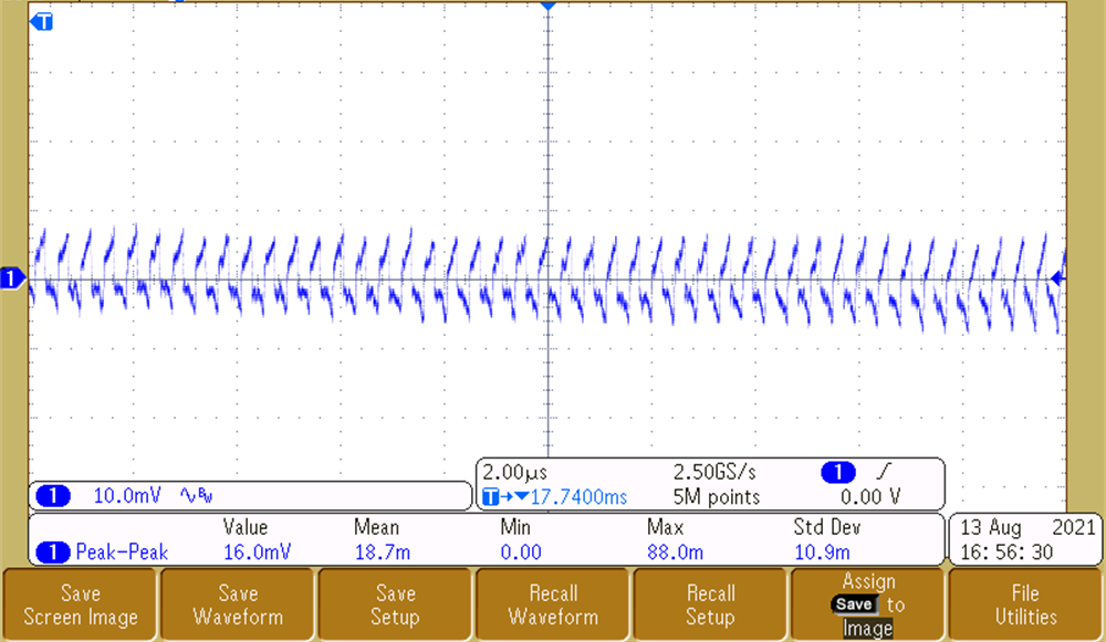
GUID-20211020-SS0I-P9CN-S2FB-QWMQZ58TV5TN-low.pngFigure 3-6 Output Voltage Ripple - 3.8 V
GUID-20211020-SS0I-HDZV-1SXR-FM63NDVLK1DF-low.pngFigure 3-8 Output Voltage Ripple - 1.8 V
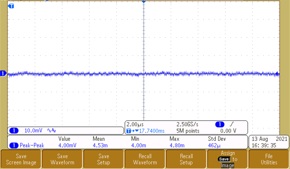
GUID-20211020-SS0I-G99F-GJJW-QJC8FNDS2FTG-low.pngFigure 3-7 Output Voltage Ripple - 3.3 V
GUID-20211020-SS0I-CGT5-4NBV-VNFBDTWLDN6H-low.pngFigure 3-9 Output Voltage Ripple - 1.1 V