TIDUBF0 January   2022


  1.   Description
  2.   Resources
  3.   Features
  4.   Applications
  5.   5
  6. 1System Description
    1. 1.1 Key System Specifications
  7. 2System Overview
    1. 2.1 Block Diagram
    2. 2.2 Design Considerations
      1. 2.2.1 PCB and Form Factor
      2. 2.2.2 Power Supply Design
        1. 2.2.2.1 POC Filter
        2. 2.2.2.2 Power Supply Considerations
          1. 2.2.2.2.1 Choosing External Components
          2. 2.2.2.2.2 Choosing the Buck 1 Inductor
          3. 2.2.2.2.3 Choosing the Buck 2 and Buck 3 Inductors
        3. 2.2.2.3 Functional Safety
    3. 2.3 Highlighted Products
      1. 2.3.1 OX01F10 Imager
      2. 2.3.2 DS90UB933-Q1
      3. 2.3.3 TPS650320-Q1
    4. 2.4 System Design Theory
  8. 3Hardware, Testing Requirements, and Test Results
    1. 3.1 Hardware Requirements
      1. 3.1.1 Hardware Setup
      2. 3.1.2 FPD-Link III I2C Initialization
      3. 3.1.3 OX01F10 Initialization
    2. 3.2 Test Setup
      1. 3.2.1 Power Supplies Start Up
      2. 3.2.2 Setup for Verifying I2C Communications
    3. 3.3 Test Results
      1. 3.3.1 Power Supplies Start-Up
      2. 3.3.2 Power Supply Start-Up—1.8-V Rail and PDB
      3. 3.3.3 Power Supply Voltage Ripple
      4. 3.3.4 Power Supply Load Currents
      5. 3.3.5 I2C Communications
  9. 4Design and Documentation Support
    1. 4.1 Design Files
      1. 4.1.1 Schematics
      2. 4.1.2 Bill of Materials
      3. 4.1.3 PCB Layout Recommendations
        1. 4.1.3.1 Layout Prints
        2. 4.1.3.2 PMIC Layout Recommendations
        3. 4.1.3.3 Serializer Layout Recommendations
        4. 4.1.3.4 Imager Layout Recommendations
        5. 4.1.3.5 PCB Layer Stackup Recommendations
      4. 4.1.4 Altium Project
      5. 4.1.5 Gerber Files
  10. 5Tools and Software
  11. 6Documentation Support
  12. 7Support Resources
  13. 8Trademarks

PCB Layer Stackup Recommendations

Figure 4-2 shows the 8-layer stackup used for the PMIC and serializer board. Two signal layers are required due to the complex routing requirements introduced by the small size requirements of the PCB that must include I2C, logic IOs, clock, and control signals between the PMIC, serializer, and imager. The separation of the outer layers is selected to ensure a characteristic impedance of 50 Ω, ±10%

In this design, high current components are placed on both the top layer and the bottom layer, so Layer 2 and Layer 7 in the stackup are dedicated ground planes to minimize high current return paths. A separate AGND plane is also included on Layer 7 for the imager.
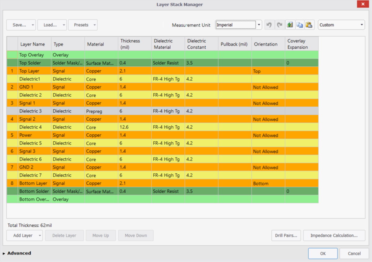
GUID-20211020-SS0I-4KWV-TF2N-DZRTJLHKTWQF-low.png Figure 4-2 Layer Stackup