TIDUC99 August   2022 TPSM82903


  1.   Description
  2.   Resources
  3.   Features
  4.   Applications
  5.   5
  6. 1System Description
  7. 2System Overview
    1. 2.1 Block Diagram
    2. 2.2 Design Considerations
    3. 2.3 Highlighted Products
    4. 2.4 System Design Theory
      1. 2.4.1 Buck Converter Circuit Design Using TPSM82903
  8. 3Hardware, Software, Testing Requirements, and Test Results
    1. 3.1 Hardware Requirements
    2. 3.2 Test Setup
    3. 3.3 Test Results
      1. 3.3.1 Startup
      2. 3.3.2 Shutdown
      3. 3.3.3 Load Transient
      4. 3.3.4 Output Ripple
      5. 3.3.5 Efficiency
      6. 3.3.6 Thermal Performance
      7. 3.3.7 Output Voltage vs. Output Current
  9. 4Design and Documentation Support
    1. 4.1 Design Files
      1. 4.1.1 Schematics
      2. 4.1.2 BOM
      3. 4.1.3 PCB Layout Recommendations
        1. 4.1.3.1 Layout Prints
      4. 4.1.4 Altium Project
      5. 4.1.5 Gerber Files
      6. 4.1.6 Assembly Drawings
    2. 4.2 Documentation Support
    3. 4.3 Support Resources
    4. 4.4 Trademarks

Load Transient

Figure 3-4 shows the transient response from 0.5-A to 3-A with 12-V input.
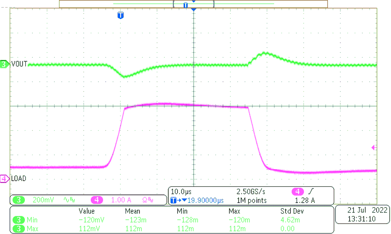
GUID-20220725-SS0I-KXPP-JGK6-VW2D8JQXJSQH-low.png Figure 3-4 Load Transient 500-mA to 3-A with 12-Vin

Figure 3-5 shows the transient response from 0.5-A to 2-A with 12-V input.
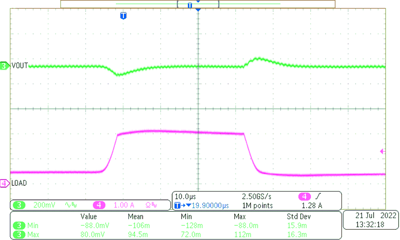
GUID-20220725-SS0I-MRLM-QHSV-FNWZGT6ZHF2K-low.png Figure 3-5 Load Transient 500-mA to 2-A with 12-Vin

Figure 3-6 shows the transient response from 0.5-A to 1-A with 12-V input.
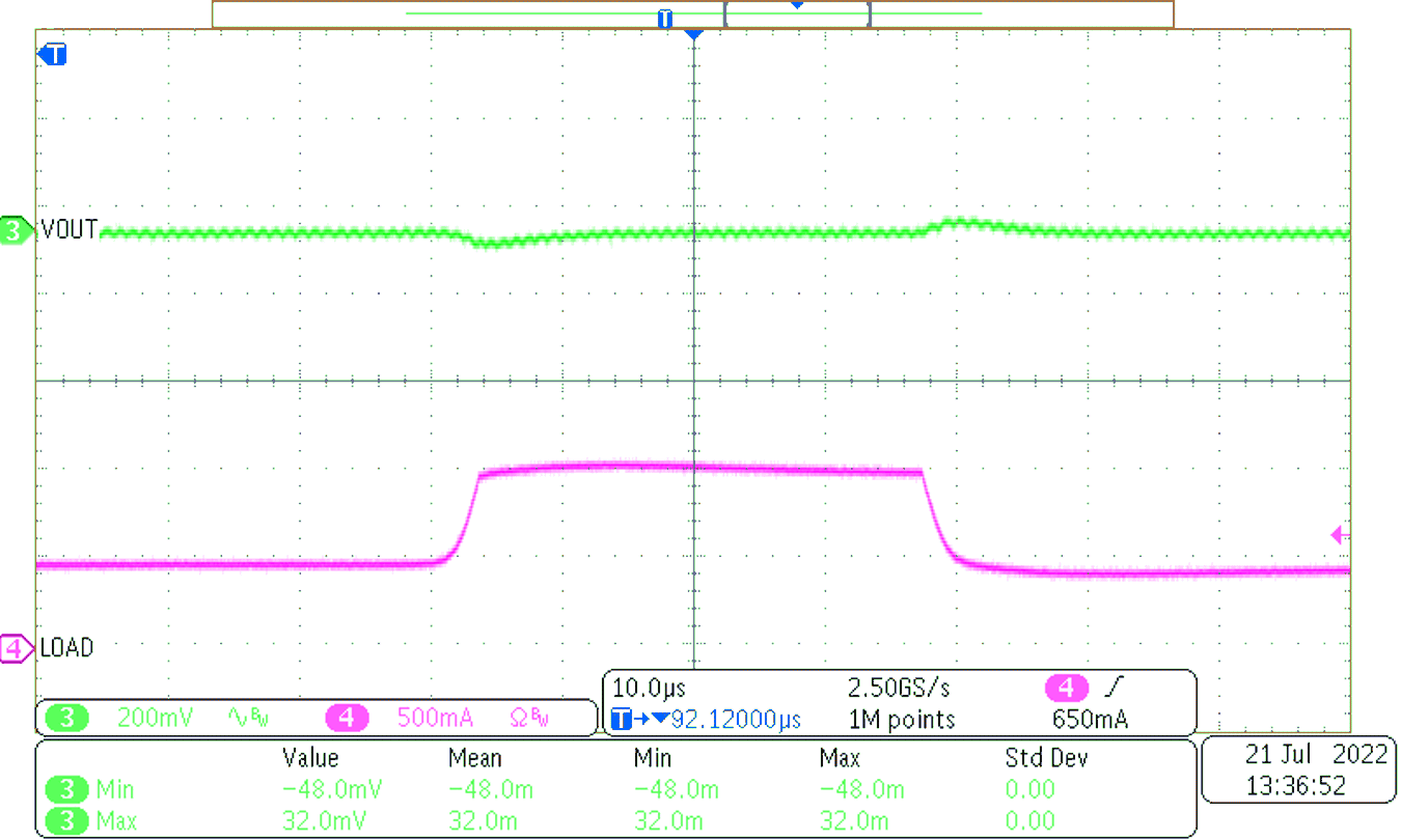
GUID-20220725-SS0I-ND94-HKZX-4F62W2DMJHXQ-low.png Figure 3-6 Load Transient 500-mA to 1-A with 12-Vin

A sinusoidal load is applied with 12-Vin. Figure 3-7 shows the transition between Power Save Mode (PSM) during light load to Pulse Width Modulation (PWM) mode at heavy load.
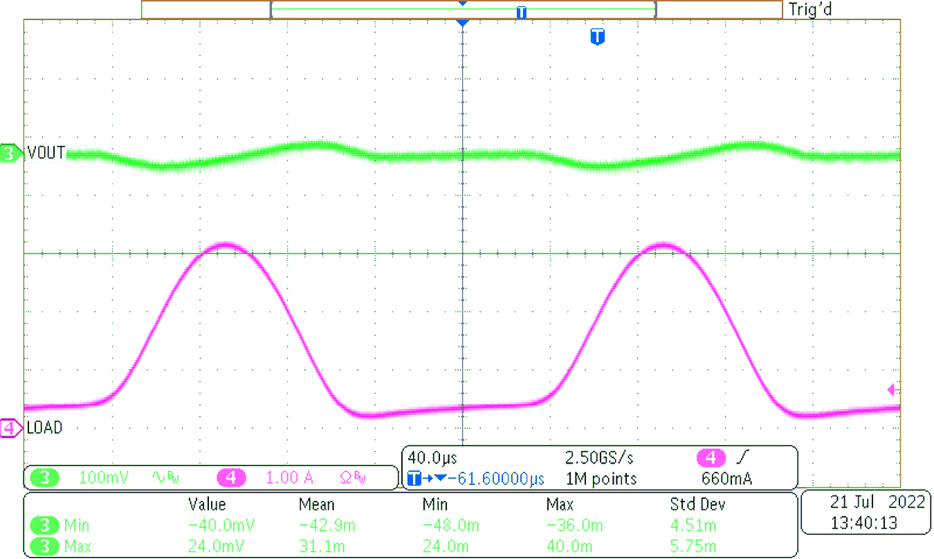
GUID-20220725-SS0I-GTZH-XM3D-NC0PT65QM2JB-low.png Figure 3-7 PSM to PWM Transition with 12-Vin