TIDUCF7 May 2022 TPSI3050 , TPSI3050-Q1 , TPSI3052 , TPSI3052-Q1
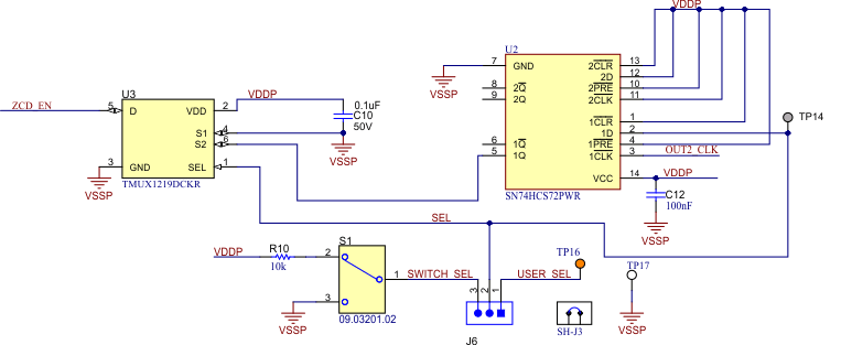
2.3.3 SN74HCS72 and TMUX1219
The SN74HCS72 is a dual D-type flip-flop (DFF) with negative-edge-triggered clock inputs. This device is part of the HCS logic family, which includes Schmitt-trigger architecture on all input pins improving noise margins and dynamic power consumption. Additionally, the HCS family provides some of the lowest static power consumption and input leakage current on the market.
SN74HCS72 features:
- Wide operating voltage range: 2 V to 6 V
- Extended ambient temperature range: –40°C to +125°C, TA
- Schmitt-trigger input architecture supports slow input transitions and improves noise margins
- Low power consumption with typical static ICC of 100 nA
- 8 ns typical delay with 5-V supply
The SN74HCS72 DFF provides the negative edge detection with a very short delay to control the switch immediately when the zero crossing is detected by the AMC23C10 comparator. The push-pull output provides excellent drive strength to control the TPSI3050-Q1 enable signal.
The flip-flop detects the falling edge of OUT2 from AMC23C10 effectively detecting the zero voltage cross. Since the design detects only the falling edge of OUT2, then the circuit has a max delay of a full cycle of the 60 Hz source or 17 ms max. Switch S1 is used in combination with TMUX1219 to enable or disable the zero cross switching circuit. Table 2-1 shows the logic of the circuit based on the states of S1, EN, OUT2, and 1Q.
This circuit detects zero cross voltage while the back to back FETs are disabled. Once the FETs are enabled, the anti-parallel diodes would not be biased to detect a zero cross voltage. If S1 is asserted low, the zero cross detection circuit is disabled. The Flip-Flop will only change state when OUT2 is changing from high to low.
If TPSI3050-Q1 is disabled, S1 is high, and OUT2 changes from low to high, only then TPSI3050-Q1 asserts VDRV high. Once VDRV is asserted high, then the FETs are turned ON.
| SEL | OUT2_CLK | 1Q | ZCD_EN | TPSI3050-Q1 State |
|---|---|---|---|---|
| L | L | L | L | Disabled |
| H | H->L | H | 1Q | Enabled |
| H | L | H | 1Q | Enabled |
| L | L->H | L | L | Disabled |
 Figure 2-5 Flip-Flop and Multiplexer
Circuit