TIDUCL0 January 2017
- 1 Description
- 2 Resources
- 3 Features
- 4 Applications
- 5 Design Images
- 6 System Overview
-
7 System Design Theory
- 7.1 Power Stage Design—Battery Power Input to the Board
- 7.2 Power Stage Design—Three-Phase Inverter
- 7.3 Power Stage Design—DRV8323 Gate Driver
- 7.4 Power Stage Design—18-V to 3.3-V DC-DC Converter
- 7.5 Power Stage Design —Microcontroller MSP430
- 7.6 Power Stage Design—Hall Sensor Interface
- 7.7 Temperature Sensing
- 7.8 Power Stage Design—External Interface Options and Indications
- 8 Getting Started Hardware and Software
- 9 Testing and Results
- 10Design Files
- 11Software Files
- 12Related Documentation
- 13Terminology
- 14About the Author
9.2.6.1 Cycle-by-Cycle Stall Current Protection by DRV8323 VDS Sensing
Figure 45 shows the test setup to simulate a stall current when the motor is rotating. S1 is a single-throw, double-pole switch connected between the motor terminals. This is used to create a motor winding to winding short.
Before S1 is closed, the motor was rotating at a steady speed. Figure 46 shows the waveforms obtained when the switch S1 is closed. When S1 is closed, S1 carries the short-circuit current. During this condition the motor stops, which causes the Hall state to continue at the current commutation state; therefore, the controller continues to generate the PWM corresponding to this commutation state.
The VDS reference for stall current limit is set to 0.1 V.
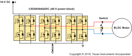 Figure 45. Test Setup to Simulate Stall Current When Motor is Running
 With the VDS reference of 0.1 V and considering a 1-mΩ RDS_ON / FET and with two FETs in parallel, set current limit = 0.1 / 0.0005 = 200 A
Figure 47 shows a zoomed view of Figure 46, the cycle-by-cycle overcurrent protection acted at around 178 A. Once the current hits 178 A, the PWM shuts off immediately, and the response time is less than 1 µs.
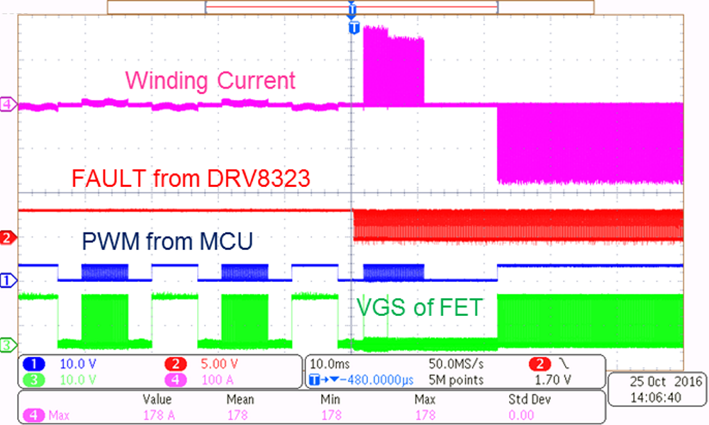 Figure 46. Cycle-by-Cycle Overcurrent Protection With Motor Stall
 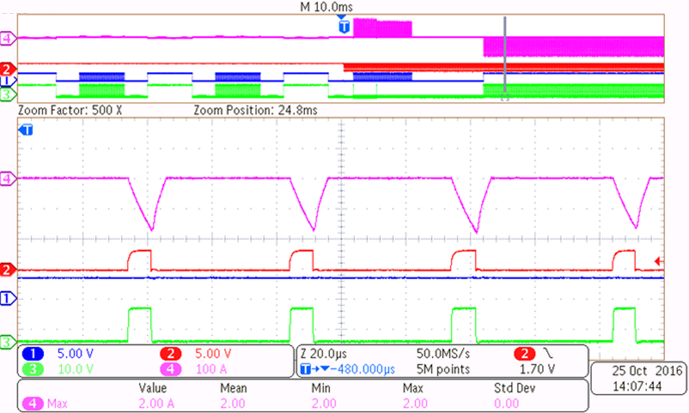 Figure 47. Zoomed View of Cycle-by-Cycle Overcurrent Protection With Motor Stall
 Figure 48 shows the test setup to simulate a short circuit at the inverter output.
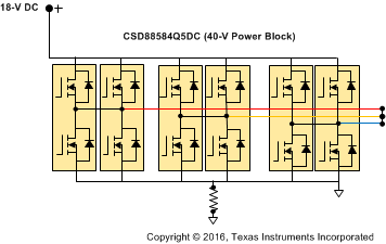 Figure 48. Test Setup to Simulate Inverter Short Circuit
 The VDS reference for short circuit is set to 0.1 V. Figure 49 shows the overcurrent protection acted at around 186 A. Once the current hits 186 A, the PWM shuts off immediately and the response time is less than 1 µs.
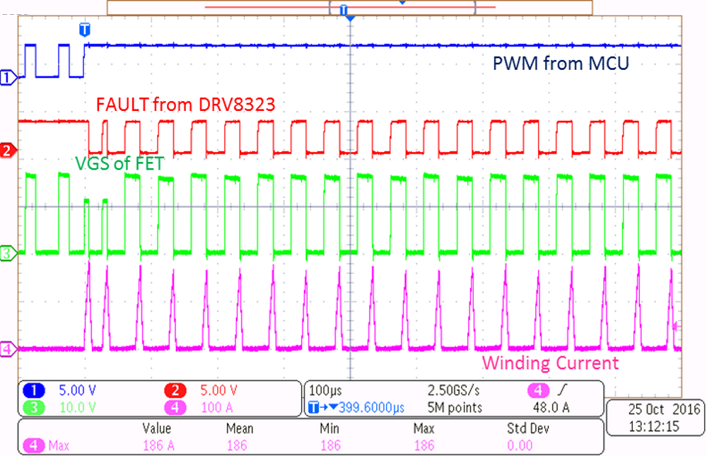 Figure 49. Cycle-by-cycle Overcurrent Protection With Inverter Output Shorted