TIDUCL0 January   2017


  1. Description
  2. Resources
  3. Features
  4. Applications
  5. Design Images
  6. System Overview
    1. 6.1 System Description
    2. 6.2 Key System Specifications
    3. 6.3 Block Diagram
    4. 6.4 Highlighted Products
      1. 6.4.1 CSD88584Q5DC
      2. 6.4.2 DRV8323
      3. 6.4.3 MSP430F5132
      4. 6.4.4 TPS54061
      5. 6.4.5 LMT87
  7. System Design Theory
    1. 7.1 Power Stage Design—Battery Power Input to the Board
    2. 7.2 Power Stage Design—Three-Phase Inverter
      1. 7.2.1 Design Considerations in Paralleling MOSFETs
        1. 7.2.1.1 Conduction Phase
        2. 7.2.1.2 Switching Phase
      2. 7.2.2 Selecting the Sense Resistor
    3. 7.3 Power Stage Design—DRV8323 Gate Driver
      1. 7.3.1 Gate Drive Features of DRV8323
      2. 7.3.2 Current Shunt Amplifier in DRV8323
      3. 7.3.3 Protection Features in DRV8323
    4. 7.4 Power Stage Design—18-V to 3.3-V DC-DC Converter
    5. 7.5 Power Stage Design —Microcontroller MSP430
    6. 7.6 Power Stage Design—Hall Sensor Interface
    7. 7.7 Temperature Sensing
    8. 7.8 Power Stage Design—External Interface Options and Indications
      1. 7.8.1 Speed Control of Motor
      2. 7.8.2 Direction of Rotation—Digital Input
      3. 7.8.3 LED Indications
      4. 7.8.4 Signal Interface Connector for External Monitoring and Control
  8. Getting Started Hardware and Software
    1. 8.1 Hardware
      1. 8.1.1 Connector Configuration of TIDA-00774
      2. 8.1.2 Programming of MSP430
      3. 8.1.3 Procedure for Board Bring-up and Testing
    2. 8.2 Software
      1. 8.2.1 System Features
      2. 8.2.2 Customizing the Reference Code
        1. 8.2.2.1 PWM_PERIOD
        2. 8.2.2.2 MAX_DUTYCYCLE
        3. 8.2.2.3 MIN_DUTYCYCLE
        4. 8.2.2.4 ACCEL_RATE
        5. 8.2.2.5 Block_Rotor_Duration
      3. 8.2.3 Configuring the DRV8323 Registers (drv8323.c)
      4. 8.2.4 Initializing SPI Communication Between DRV8323 and MSP430 (drv8323.h)
      5. 8.2.5 Running Project in Code Composer Studio (CCS)
  9. Testing and Results
    1. 9.1 Test Setup
    2. 9.2 Test Data
      1. 9.2.1 Functional Tests
        1. 9.2.1.1 3.3-V Power Supply Generated by Step-Down Converter
        2. 9.2.1.2 Gate Drive Voltage Generated by Gate Driver
        3. 9.2.1.3 Dead Time From DRV8323
        4. 9.2.1.4 MOSFET Switching Waveforms
        5. 9.2.1.5 VGS Skew of Parallel FETs During Switching
      2. 9.2.2 Load Test
        1. 9.2.2.1 Load Test Without Heat Sink
        2. 9.2.2.2 Load Test With Heat Sink
        3. 9.2.2.3 Load Test With Heat Sink and Airflow
      3. 9.2.3 Inverter Efficiency Test
      4. 9.2.4 Thermal Rise at Different Power Levels
      5. 9.2.5 Inverter Current Sensing by VDS Monitoring
      6. 9.2.6 Overcurrent and Short-Circuit Protection Test
        1. 9.2.6.1 Cycle-by-Cycle Stall Current Protection by DRV8323 VDS Sensing
        2. 9.2.6.2 Stall Current Latch Protection by DRV8323 VDS Sensing
      7. 9.2.7 Testing for Peak Current Capability
  10. 10Design Files
    1. 10.1 Schematics
    2. 10.2 Bill of Materials
    3. 10.3 PCB Layout Recommendations
      1. 10.3.1 Layout Prints
    4. 10.4 Altium Project
    5. 10.5 Gerber Files
    6. 10.6 Assembly Drawings
  11. 11Software Files
  12. 12Related Documentation
    1. 12.1 Trademarks
  13. 13Terminology
  14. 14About the Author

Speed Control of Motor

The speed control is done using a potentiometer (POT), and the POT voltage is fed to the ADC of the MCU. The circuit is shown in Figure 11. The POT is supplied from the 3.3 V. A 20k POT can be connected externally to the jumper J1. Connect the fixed terminals of the POT to terminal 1 and 3 of J1 and mid-point to terminal 2 of J1.
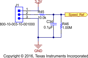
TIDA-00774 tida-00774-schematic-temperature-sensor.gifFigure 11. Potentiometer Connection for Speed Control Schematic

The resistor R46 is used to ensure that the speed control reference is zero if the POT terminal is open.