TIDUCL0 January   2017


  1. Description
  2. Resources
  3. Features
  4. Applications
  5. Design Images
  6. System Overview
    1. 6.1 System Description
    2. 6.2 Key System Specifications
    3. 6.3 Block Diagram
    4. 6.4 Highlighted Products
      1. 6.4.1 CSD88584Q5DC
      2. 6.4.2 DRV8323
      3. 6.4.3 MSP430F5132
      4. 6.4.4 TPS54061
      5. 6.4.5 LMT87
  7. System Design Theory
    1. 7.1 Power Stage Design—Battery Power Input to the Board
    2. 7.2 Power Stage Design—Three-Phase Inverter
      1. 7.2.1 Design Considerations in Paralleling MOSFETs
        1. 7.2.1.1 Conduction Phase
        2. 7.2.1.2 Switching Phase
      2. 7.2.2 Selecting the Sense Resistor
    3. 7.3 Power Stage Design—DRV8323 Gate Driver
      1. 7.3.1 Gate Drive Features of DRV8323
      2. 7.3.2 Current Shunt Amplifier in DRV8323
      3. 7.3.3 Protection Features in DRV8323
    4. 7.4 Power Stage Design—18-V to 3.3-V DC-DC Converter
    5. 7.5 Power Stage Design —Microcontroller MSP430
    6. 7.6 Power Stage Design—Hall Sensor Interface
    7. 7.7 Temperature Sensing
    8. 7.8 Power Stage Design—External Interface Options and Indications
      1. 7.8.1 Speed Control of Motor
      2. 7.8.2 Direction of Rotation—Digital Input
      3. 7.8.3 LED Indications
      4. 7.8.4 Signal Interface Connector for External Monitoring and Control
  8. Getting Started Hardware and Software
    1. 8.1 Hardware
      1. 8.1.1 Connector Configuration of TIDA-00774
      2. 8.1.2 Programming of MSP430
      3. 8.1.3 Procedure for Board Bring-up and Testing
    2. 8.2 Software
      1. 8.2.1 System Features
      2. 8.2.2 Customizing the Reference Code
        1. 8.2.2.1 PWM_PERIOD
        2. 8.2.2.2 MAX_DUTYCYCLE
        3. 8.2.2.3 MIN_DUTYCYCLE
        4. 8.2.2.4 ACCEL_RATE
        5. 8.2.2.5 Block_Rotor_Duration
      3. 8.2.3 Configuring the DRV8323 Registers (drv8323.c)
      4. 8.2.4 Initializing SPI Communication Between DRV8323 and MSP430 (drv8323.h)
      5. 8.2.5 Running Project in Code Composer Studio (CCS)
  9. Testing and Results
    1. 9.1 Test Setup
    2. 9.2 Test Data
      1. 9.2.1 Functional Tests
        1. 9.2.1.1 3.3-V Power Supply Generated by Step-Down Converter
        2. 9.2.1.2 Gate Drive Voltage Generated by Gate Driver
        3. 9.2.1.3 Dead Time From DRV8323
        4. 9.2.1.4 MOSFET Switching Waveforms
        5. 9.2.1.5 VGS Skew of Parallel FETs During Switching
      2. 9.2.2 Load Test
        1. 9.2.2.1 Load Test Without Heat Sink
        2. 9.2.2.2 Load Test With Heat Sink
        3. 9.2.2.3 Load Test With Heat Sink and Airflow
      3. 9.2.3 Inverter Efficiency Test
      4. 9.2.4 Thermal Rise at Different Power Levels
      5. 9.2.5 Inverter Current Sensing by VDS Monitoring
      6. 9.2.6 Overcurrent and Short-Circuit Protection Test
        1. 9.2.6.1 Cycle-by-Cycle Stall Current Protection by DRV8323 VDS Sensing
        2. 9.2.6.2 Stall Current Latch Protection by DRV8323 VDS Sensing
      7. 9.2.7 Testing for Peak Current Capability
  10. 10Design Files
    1. 10.1 Schematics
    2. 10.2 Bill of Materials
    3. 10.3 PCB Layout Recommendations
      1. 10.3.1 Layout Prints
    4. 10.4 Altium Project
    5. 10.5 Gerber Files
    6. 10.6 Assembly Drawings
  11. 11Software Files
  12. 12Related Documentation
    1. 12.1 Trademarks
  13. 13Terminology
  14. 14About the Author

Stall Current Latch Protection by DRV8323 VDS Sensing

The same test setup in Figure 45 is used for the stall current protection. The VDS reference used is 0.1 by writing in the register of the DRV8323. The latch protection acted at 143 A.

Figure 50 shows the test results with latch protection by VDS sensing. When a VDS overcurrent event occurs, the device will pull all gate drive outputs low to put all six external MOSFETs into high impedance mode. The fault will be reported on the nFAULT pin with the specific MOSFET in which the overcurrent event was detected is reported through the SPI status registers. Figure 51 shows the zoomed view of Figure 50.
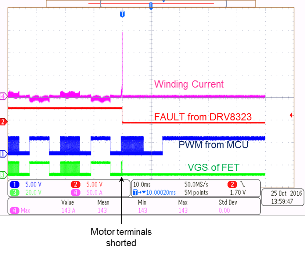
TIDA-00774 tida-00774-overcurrent-latch-protection-with-motor-stall-by-VDS-sensing.pngFigure 50. Overcurrent Latch Protection With Motor Stall by VDS Sensing
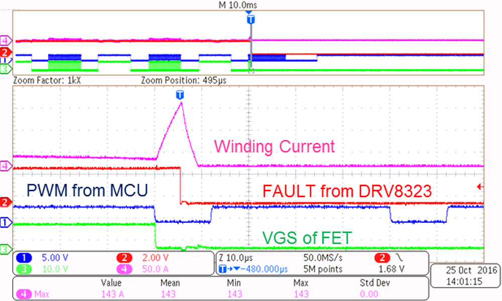
TIDA-00774 tida-00774-overcurrent-latch-protection-with-motor-stall-by-VDS-sensing-zoomed.pngFigure 51. Zoomed View of Overcurrent Latch Protection With Motor Stall by VDS Sensing

Figure 52 shows the test results of latch protection, when the inverter output is shorted. The same test setup in Figure 48 is used for the short-circuit simulation. The VDS reference used is 0.1 V. The latch protection acted at 144 A.
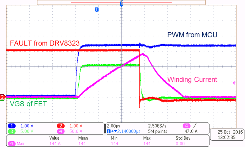
TIDA-00774 tida-00774-overcurrent-latch-protection-with-inverter-output-shorted.pngFigure 52. Overcurrent Latch Protection With Inverter Output Shorted