TIDUED7A November 2018 – November 2022
2.3.1 PCB and Form Factor
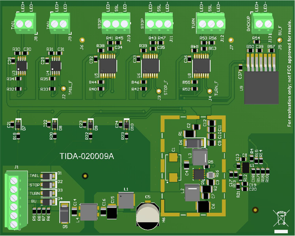
This reference design uses a two-layer printed circuit board (PCB) with 1.5 oz of copper where all components are placed on the top layer. The PCB is not intended to fit any particular form factor and has a dimension of 88 mm × 70 mm. The primary objective of the design with regards to the PCB is to make a solution that is compact while still providing a way to test the performance of the board. In a final-production version of this reference design, the size of the solution can be further reduced. Figure 2-4 shows a 3D rendering of the PCB.
 Figure 2-4 3D Render of TIDA-020009 PCB