TIDUEJ8C January 2019 – May 2024
- 1
- Description
- Resources
- Features
- Applications
- 6
- 1System Description
- 2System Overview
- 3Hardware, Software, Testing Requirements, and Test Results
- 4Design Files
- 5Related Documentation
- 6About the Author
- 7Revision History
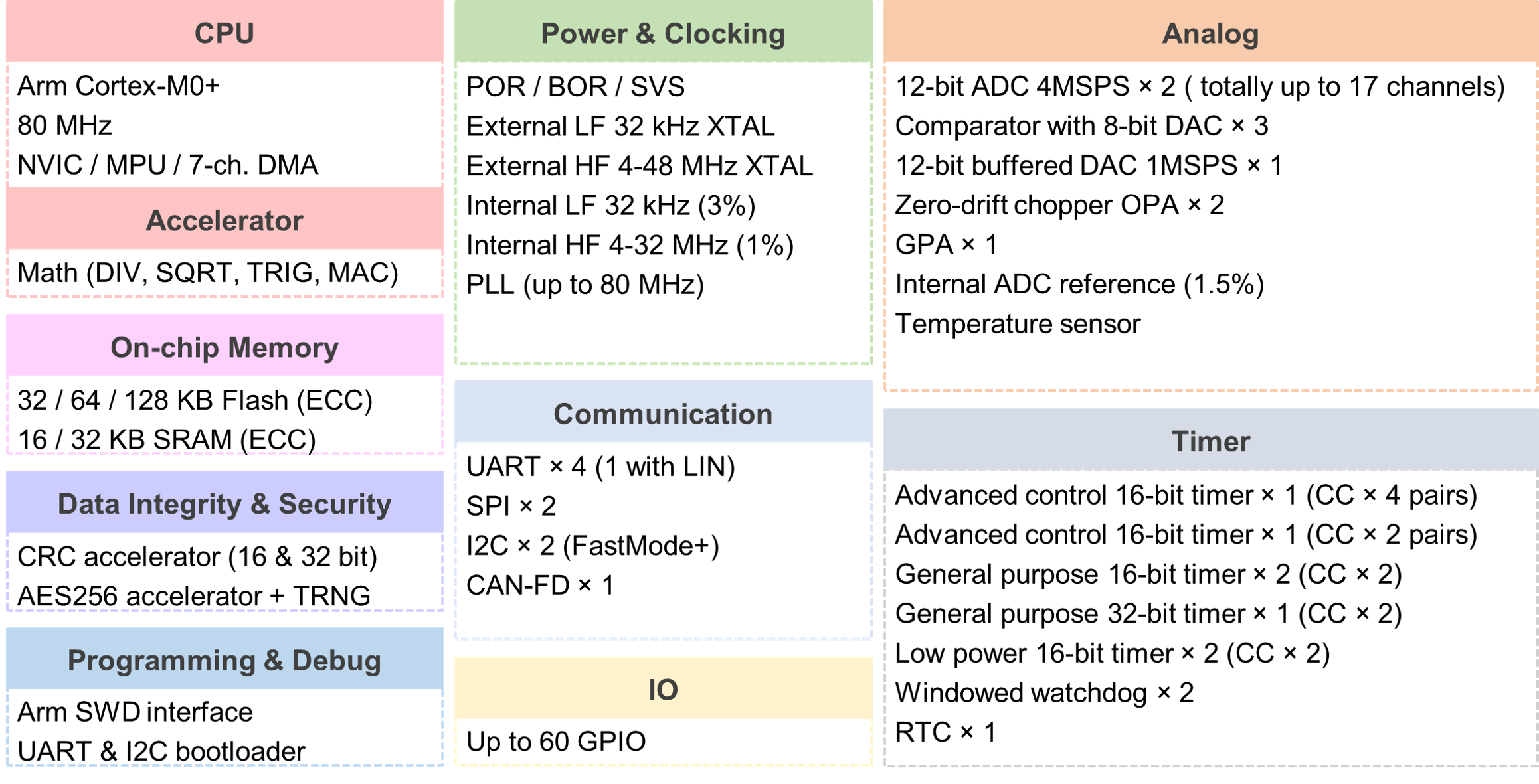
2.3.1 MSPM0G1506
 Figure 2-2 MSPM0G1506 Block Diagram
The MSPM0G1506 is an 80MHz MCU with seven timers support up to 22 PWM channels, 64KB flash, 32KB RAM, two 12-bit 4-MSPS ADC, two zero-drift zero-crossover chopper op-amps, three high-speed comparators with 8-bit reference DACs and a 12-bit 1-MSPS DAC with integrated output buffer.
- Wide supply voltage range: 1.62V to 3.6V
- Optimized low-power modes
- RUN: 96µA/MHz (CoreMark)
- SLEEP: 458µA at 4MHz
- STOP: 47µA at 32kHz
- STANDBY: 1.5µA with RTC and SRAM retention
- SHUTDOWN: 78nA with IO wake-up capability
- 32-Bit Cortex-M0+ platform with a holistic ultra-low-power system architecture
- Flexible Power-Management System
- Internally regulated core supplies
- Supply Voltage Supervision, Monitoring, and Brownout
- Clock System
- Internal 4- to 32MHz oscillator with up to ±1.2% accuracy (SYSOSC)
- Phase-locked loop (PLL) up to 80MHz
- Internal 32kHz low-frequency oscillator (LFOSC) with ±3% accuracy
- External 4- to 48MHz crystal oscillator (HFXT)
- External 32kHz crystal oscillator(LFXT)
- External clock input
- Math accelerator supports DIV, SQRT, MAC and TRIG computations
- 7-Channel DMA controller
- Up to 60 GPIOs, Two high-drive IOs with 20mA drive, Two 5V tolerant IOs
- Timers
- Two 16-bit advanced timers with deadband support up to 12 PWM channels
- One 32-bit high-resolution general-purpose timer
- Two 16-bit general-purpose timers support low-power operation in STANDBY mode
- One 16-bit general-purpose timer supports QEI
- One 16-bit general-purpose timer
- Four UART interfaces; one supports LIN, IrDA, DALI, Smart Card, Manchester, and three support low-power operation in STANDBY mode
- Two I2C interfaces support up to FM+ (1Mbit/s), SMBus/PMBus, and wakeup from STOP mode
- Two SPIs, one SPI supports up to 32Mbits/s
- Two simultaneous sampling 12-bit 4Msps ADCs
- 14-bit effective resolution at 250ksps with hardware averaging
- 12-bit output resolution at 4Msps with greater than 11 ENOB
- Up to 17 total external input channels with individual result storage registers
- Internal channels for temperature sensing, supply monitoring, and analog signal chain (interconnection with OPA, DAC, etc.)
- Software selectable reference
- Operates in RUN, SLEEP, and STOP modes
- Three high-speed comparators (COMP) with 8-bit reference DACs
- Programmable hysteresis
- Programmable reference voltage
- Configurable operation modes
- Programmable output glitch filter delay
- Supports 6 blanking sources
- Output connected to advanced timer fault handling mechanism
- Supports TI System Configuration Tool
The voltage and current of the panel and battery lines are used to calculate and track the MPP and the MSPM0G1506 enables quick data acquisition from the various analog signals using the internal analog-to-digital converter (ADC). Operating at 80MHz allows for fast conversion and calculation to efficiently perform MPPT and adjust the duty cycle of buck converter accordingly.
During battery charging mode, the MSPM0G1506 generates pulse-width modulated (PWM) signals to the buck converter, where the duty cycle is proportional to the output current, or battery charging current, of the buck stage. The MCU is also responsible for managing the battery voltage by preventing over-charging of the battery. The MCU does this by turning the converter into constant voltage mode once a threshold voltage is reached. Additionally, the MCU protects the battery from over-discharging by disconnecting the load once a threshold load current is reached or once the battery voltage falls below another threshold. By effectively managing the battery, this reference design maximizes the lifespan and optimizes the performance capabilities.
Status indicators and alarms, controlled by the MCU, are also included in the design to provide feedback to the user; however, some are left uninitialized.