TIDUEJ8C January 2019 – May 2024
- 1
- Description
- Resources
- Features
- Applications
- 6
- 1System Description
- 2System Overview
- 3Hardware, Software, Testing Requirements, and Test Results
- 4Design Files
- 5Related Documentation
- 6About the Author
- 7Revision History
3.1.1.1 TIDA-010042
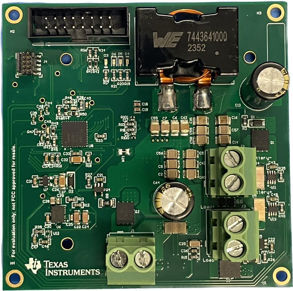
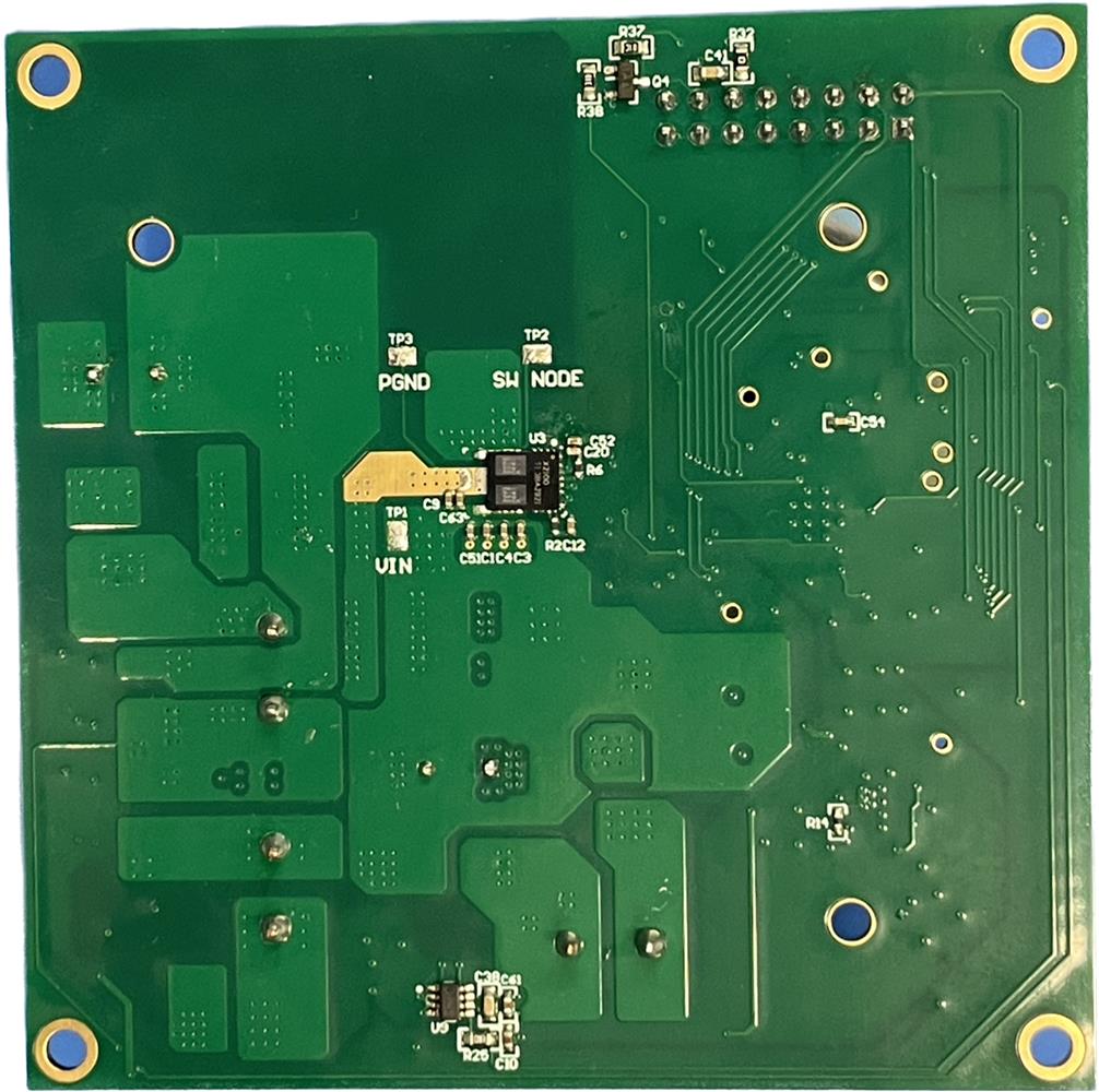
Figure 3-1 and Figure 3-2 show the full design boards, with the bare PCB measuring at 83mm × 82mm.
 Figure 3-1 TIDA-010042 Top View
 Figure 3-2 TIDA-010042 Bottom View
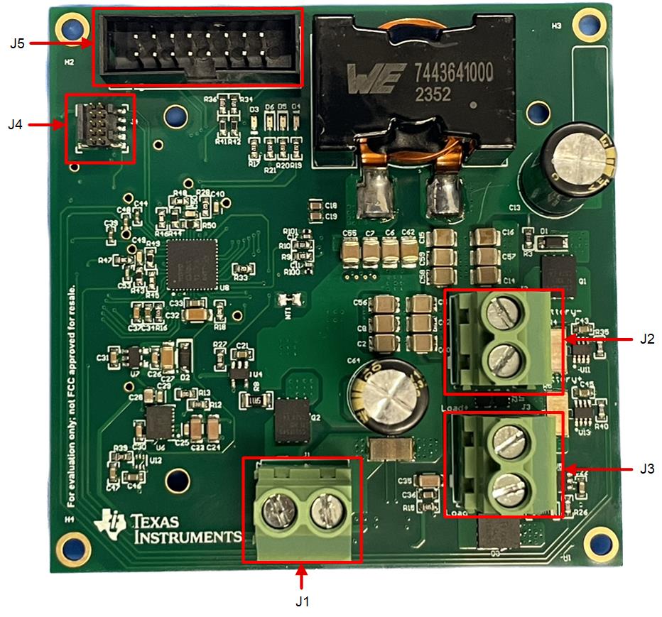
Table 3-1 breaks out the various headers and their associated pin connections.
J1, J2, and J3 are the PV panel, battery, and load connections, respectively.
J4 is used for XDS110 debugger.
J5 can be configured to communicate with power line communication (PLC) board in the future.
 Figure 3-3 TIDA-010042 Board Headers
Table 3-1 Headers Connections
| DESIGNATOR | PIN NUMBER | SIGNAL |
|---|---|---|
| J1 – PV panel connection | 1 | Negative panel (P–) terminal |
| 2 | Positive panel (P+) terminal | |
| J2 – battery connection | 1 | Positive battery (B+) terminal |
| 2 | Negative battery (B–) terminal | |
| J3 – load connection | 1 | Negative load (L–) terminal |
| 2 | Positive load (L+) terminal | |
| J4 – programming header | 1 | XDS110 Programmer voltage |
| 2 | XDS110 SWDIO | |
| 3 | GROUND | |
| 4 | XDS110 SWCLK | |
| 5 | GROUND | |
| 6 | FLOAT | |
| 7 | GROUND | |
| 8 | FLOAT | |
| 9 | GROUND | |
| 10 | XDS110 RST | |
| J5 – PLC connection | 1 | PLC1 |
| 2 | PLC2 | |
| 3 | PLC3 | |
| 4 | PLC4 | |
| 5 | PLC5 | |
| 6 | PLC6 | |
| 7 | PLC7 | |
| 8 | PLC8 | |
| 9 | PLC9 | |
| 10 | PLC10 | |
| 11 | UART_TX | |
| 12 | POWER 3.3V | |
| 13 | UART_RX | |
| 14 | Buzzer output | |
| 15 | GROUND | |
| 16 | GROUND |