TIDUEM7A April   2019  – February 2021


  1.   Description
  2.   Resources
  3.   Features
  4.   Applications
  5.   5
  6. 1System Description
    1. 1.1 End Equipment
      1. 1.1.1 Electricity Meter
    2. 1.2 Key System Specifications
  7. 2System Overview
    1. 2.1 Block Diagram
    2. 2.2 Highlighted Products
      1. 2.2.1 ADS131M04
      2. 2.2.2 TPS7A78
      3. 2.2.3 MSP432P4111
      4. 2.2.4 TPS3840
      5. 2.2.5 THVD1500
      6. 2.2.6 ISO7731B
      7. 2.2.7 TRS3232E
      8. 2.2.8 TPS709
      9. 2.2.9 ISO7720
    3. 2.3 Design Considerations
      1. 2.3.1 Design Hardware Implementation
        1. 2.3.1.1 TPS7A78 Cap-Drop Supply
        2. 2.3.1.2 TPS3840 SVS
        3. 2.3.1.3 Analog Inputs
          1. 2.3.1.3.1 Voltage Measurement Analog Front End
          2. 2.3.1.3.2 Current Measurement Analog Front End
      2. 2.3.2 Current-Detection Mode
        1. 2.3.2.1 ADS131M04 Current-Detection Procedure
        2. 2.3.2.2 Using an MCU to Trigger Current-Detection Mode
          1. 2.3.2.2.1 Using a Timer to Trigger Current-Detection Mode Regularly
          2. 2.3.2.2.2 MCU Procedure for Entering and Exiting Current-Detection Mode
        3. 2.3.2.3 How to Implement Software for Metrology Testing
          1. 2.3.2.3.1 Setup
            1. 2.3.2.3.1.1 Clock
            2. 2.3.2.3.1.2 Port Map
            3. 2.3.2.3.1.3 UART Setup for GUI Communication
            4. 2.3.2.3.1.4 Real-Time Clock (RTC)
            5. 2.3.2.3.1.5 LCD Controller
            6. 2.3.2.3.1.6 Direct Memory Access (DMA)
            7. 2.3.2.3.1.7 ADC Setup
          2. 2.3.2.3.2 Foreground Process
            1. 2.3.2.3.2.1 Formulas
          3. 2.3.2.3.3 Background Process
            1. 2.3.2.3.3.1 per_sample_dsp()
              1. 2.3.2.3.3.1.1 Voltage and Current Signals
              2. 2.3.2.3.3.1.2 Frequency Measurement and Cycle Tracking
            2. 2.3.2.3.3.2 LED Pulse Generation
            3. 2.3.2.3.3.3 Phase Compensation
    4. 2.4 Hardware, Software, Testing Requirements, and Test Results
      1. 2.4.1 Required Hardware and Software
        1. 2.4.1.1 Cautions and Warnings
        2. 2.4.1.2 Hardware
          1. 2.4.1.2.1 Connections to the Test Setup
          2. 2.4.1.2.2 Power Supply Options and Jumper Settings
        3. 2.4.1.3 Software
      2. 2.4.2 Testing and Results
        1. 2.4.2.1 Test Setup
          1. 2.4.2.1.1 SVS and Cap-Drop Functionality Testing
          2. 2.4.2.1.2 Electricity Meter Metrology Accuracy Testing
          3. 2.4.2.1.3 Current-Detection Mode Testing
          4. 2.4.2.1.4 Viewing Metrology Readings and Calibration
            1. 2.4.2.1.4.1 Viewing Results From LCD
            2. 2.4.2.1.4.2 Calibrating and Viewing Results From PC
              1. 2.4.2.1.4.2.1 Viewing Results
              2. 2.4.2.1.4.2.2 Calibration
                1. 2.4.2.1.4.2.2.1 Gain Calibration
                  1. 4.2.1.4.2.2.1.1 Voltage and Current Gain Calibration
                  2. 4.2.1.4.2.2.1.2 Active Power Gain Calibration
                2. 2.4.2.1.4.2.2.2 Offset Calibration
                3. 2.4.2.1.4.2.2.3 Phase Calibration
        2. 2.4.2.2 Test Results
          1. 2.4.2.2.1 SVS and TPS7A78 Functionality Testing Results
          2. 2.4.2.2.2 Electricity Meter Metrology Accuracy Results
          3. 2.4.2.2.3 Current-Detection Mode Results
  8. 3Design Files
    1. 3.1 Schematics
    2. 3.2 Bill of Materials
    3. 3.3 PCB Layout Recommendations
      1. 3.3.1 Layout Prints
    4. 3.4 Altium Project
    5. 3.5 Gerber Files
    6. 3.6 Assembly Drawings
  9. 4Related Documentation
    1. 4.1 Trademarks
  10. 5About the Author
  11. 6Revision History

ADS131M04

The ADS131M04 device is a four-channel, simultaneously-sampling, 24-bit, 2nd order delta-sigma (ΔΣ), analog-to-digital converter (ADC) that offers wide dynamic range, and internal calibration features making it well-suited for energy metering, power quality, and protection applications. The ADC inputs can be directly interfaced to a resistor-divider network, a transformer to measure voltage or current, a shunt to measure current, or a Rogowski coil to measure current.

The individual ADC channels can be independently configured depending on the sensor input. A low noise, programmable gain amplifier (PGA) provides gains ranging from 1 to 128 to amplify low-level signals. Additionally, these devices integrate channel-to-channel phase alignment and offset and gain calibration registers to help remove signal chain errors. A low-drift, 1.2-V reference is integrated into the device reducing printed circuit board (PCB) area. Cyclic redundancy check (CRC) options can be individually enabled on the data input, data output, and register map to ensure communication integrity. Figure 2-2 shows a block diagram of this device.
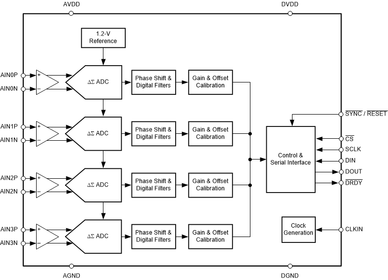
GUID-6D6BB138-3547-47C1-AAF4-06F3E08CAD9F-low.gifFigure 2-2 ADS131M04 Functional Block Diagram

In Figure 2-2, 2.7 V–3.6 V must be fed between AVDD and AGND as well as between DVDD and GND. In addition, an external clock must be connected to CLKIN. When the ADS131M04 device is configured for high-resolution mode, this clock must be between 1 MHz and 8.3 MHz for the ADS131M04 to properly work. The CLKIN clock of the ADS131M04 device can be generated from the SMCLK clock output of the MSP432 MCU. The ADS131M04 divides this clock by two and uses this divided clock for its delta-sigma modulator clock. When new ADC samples are ready, the ADS131M04 asserts its DRDY pin to alert the host MCU that there are new ADC samples available. Since the ADS131M04 device can accept a clock with a wide frequency range, the device itself can also be used for applications that require coherent sampling.