TIDUEM7A April 2019 – February 2021
- Description
- Resources
- Features
- Applications
- 5
- 1System Description
-
2System Overview
- 2.1 Block Diagram
- 2.2 Highlighted Products
- 2.3 Design Considerations
- 2.4
Hardware, Software, Testing Requirements, and Test Results
- 2.4.1 Required Hardware and Software
- 2.4.2
Testing and Results
- 2.4.2.1 Test Setup
- 2.4.2.2 Test Results
- 3Design Files
- 4Related Documentation
- 5About the Author
- 6Revision History
2.3.1.3.2 Current Measurement Analog Front End
The analog front end for current inputs is different from the analog front end for the voltage inputs. Figure 2-5 shows the analog front end used for the CT current channel, where the positive and negative leads from a CT are connected to pins 3 and 1 of header J26.
 Figure 2-5 Analog Front End for CT Current Inputs
The analog front end for current consists of footprints for electromagnetic interference filter beads (R48 and R57), burden resistors for current transformers (R51 and R56), and an RC low-pass filter (R49, R58, C52, C53, and C54) that functions as an anti-alias filter. There are also footprints (U12 and U13) that can be replaced with the TVS0500 for supplemental protection from surges, if required.
As Figure 2-5 shows, resistors R51 and R56 are the burden resistors, which are in series with each other. For best THD performance, instead of using one burden resistor, two identical burden resistors in series are used with the common point being connected to GND. This split-burden resistor configuration ensures that the waveforms fed to the positive and negative terminals of the ADC are 180 degrees out of phase with each other, which provides the best THD results with this ADC. The total burden resistance is selected based on the current range used and the turns ratio specification of the CT (this design uses CTs with a turns ratio of 2000). The total value of the burden resistor for this design is 12.98 Ω.
Equation 2 shows how to calculate the range of differential voltages fed to the current ADC channel for a given maximum current, CT turns ratio, and burden resistor value.
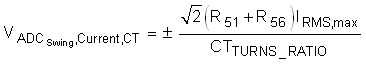
Based on the maximum current of 100 A, CT turns ratio of 2000, and burden resistor of 12.98 Ω of this design, the input signal to the current ADC has a voltage swing of ±918 mV maximum (649 mVRMS) when the maximum current rating of the meter (100 A) is applied. This ±918-mV maximum input voltage is well within the ±1.2-V input range of the device for the selected PGA gain of 1 that is used for the current channels.
Figure 2-6 shows the analog front end used for the shunt current channel, where the positive and negative leads from the shunt are connected to pins 1 and 3 of header J25. The ground connection for the shunt is connected to pin 2 of this J25 header.
 Figure 2-6
Analog Front End for Shunt Current Inputs
Figure 2-6
Analog Front End for Shunt Current InputsThe circuitry in Figure 2-6 is similar to the circuit shown for the CT channel, except the R51 and R56 burden resistors are now removed since a shunt is used instead of a CT. Since the burden resistors have been removed, do not connect a CT to this channel because it may cause a large output voltage that may damage the meter. In addition, note that the pin order of the AINxP and AINxN pins on the ADS131M04 device is swapped when going from one converter to another. As an example, AIN1N is pin 5 and AIN1P is pin 6, but AIN2P is pin 7 and AIN2N is pin 8. The swapped order is why the order of the CT positive output terminal and negative output terminal on J26 is swapped when compared to the shunt positive and negative output terminal on J25.
Equation 2 shows how to calculate the range of differential voltages fed to the current ADC channel for a given maximum current and shunt value.
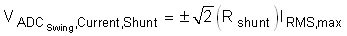
With shunt current sensors, the shunt sensor value is selected based on the tradeoff between accuracy and shunt power dissipation. If the shunt value is decreased, less power is dissipated through the shunt; however, the decreased shunt value means a smaller output voltage from the shunt, which leads to worse accuracies at lower currents, even if a higher PGA gain is used to boost the shunt output. In this design, tests are performed with both 100- and 200-µΩ shunts.
Based on the VADC,shunt range, select the proper PGA gain by looking at the full-scale range table in Table 2-1 to find the two gain ranges that VADC,shunt, shunt voltage fits between. From these two gain values, select the lower gain setting as the selected PGA gain value for the shunt channel. This gain value maximizes the ADC range without saturation occurring at higher currents. As an example of this process, suppose a 100-A maximum RMS current and a 200-µΩ shunt is used. Based on these values, VADC,shunt varies between ±28.3 mV. This voltage range is between the maximum ±37.5 mV voltage at a gain of 32 and ±18.75 mV at a PGA gain of 64 so the PGA gain setting of the shunt channel is set for 32.
| GAIN SETTING | FSR |
|---|---|
| 1 | ±1.2 V |
| 2 | ±600 mV |
| 4 | ±300 mV |
| 8 | ±150 mV |
| 16 | ±75 mV |
| 32 | ±37.5 mV |
| 64 | ±18.75 mV |
| 128 | ±9.375 mV |