TIDUES0E June 2019 – April 2024 TMS320F28P550SJ , TMS320F28P559SJ-Q1
- 1
- Description
- Resources
- Features
- Applications
- 6
- 1System Description
- 2System Overview
- 3Circuit Description
- 4Hardware, Software, Testing Requirements, and Test Results
- 5Design Files
- 6Related Documentation
- 7Terminology
- 8About the Author
- 9Revision History
4.2 Test Setup
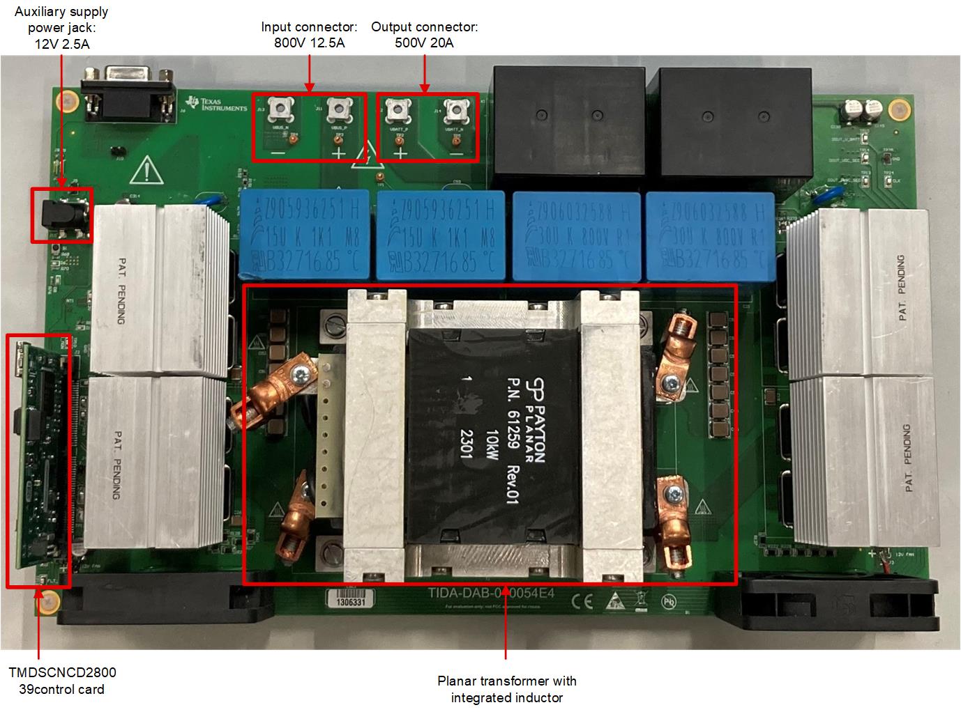
To test the efficiency of this reference design, use the setup shown in Figure 4-7.
- 10-kW DC power supply: 800 V, 12.5 A
- 10-kW resistive load: 500 V, 20 A
- Auxiliary power supply to provide 12 V, 2 .5 A
- TMDSCNCD280039C control card
- Power Analyzer
- Oscilloscope with isolated probes for voltage and current
- 12-V fans to provide sufficient airflow to the heat sinks
 Figure 4-7 Test Setup
 Figure 4-8 Board Image
Before powering the board to perform open-loop testing, use the following steps to set up the board:
- Connect the terminals J11 and J13 to the input power supply and terminals J12 and J14 to the output load bank. Use a 4-mm2 wire to make these connections so that the wire can handle high currents without getting heated quickly.
- Connect the auxiliary power supply to terminal J15 using a PJ-002 female connector to power the controller, gate driver, and sense circuits
There is a cut-out area provided at the center of the board to mount the transformer. The transformer is directly connected to the board using M3 screws. Take care while mounting the transformer so that the primary and secondary sides are not interchanged.
The control card is programmed using a USB connection from the laptop to generate PWM pulses at 100 kHz. Once programmed, the auxiliary power supply is set to 12 V. Do not apply voltage across terminals J2 and J4. In this state the current consumption on the 12-V rail is supposed to be approximately 700 mA. This consumption increases after relays are closed and fans are enabled.
Connect two 12-V fans to the fan connectors J1 and J3. The polarity is marked on the PCB and in the schematics.
Follow Lab 1 to Lab 7 to get familiar with the design and provide proper operation.
| CONNECTOR TERMINALS | FUNCTION | COMMENTS |
|---|---|---|
| J11–J13 | Input high-voltage power supply | 800-V DC power supply capable of sourcing 10-kW power |
| J12–J14 | Output load terminals | 10-kW resistive load bank is connected here |
| J15 | Auxiliary power supply for gate driver, control card, and sense circuits | 15-V DC power supply current limited to 700 mA |
| J2 | TMDSCNCD280049C Control card | Insert the control card here |
| J6 | CAN Connector | Not supported in current revision |
| J1, J3 | Fan connector | 12-V fan connectors for cooling |