TIDUES0E June   2019  – April 2024 TMS320F28P550SJ , TMS320F28P559SJ-Q1


  1.   1
  2.   Description
  3.   Resources
  4.   Features
  5.   Applications
  6.   6
  7. 1System Description
    1. 1.1 Key System Specifications
  8. 2System Overview
    1. 2.1 Block Diagram
    2. 2.2 Highlighted Products
      1. 2.2.1  UCC21710
      2. 2.2.2  UCC14141-Q1
      3. 2.2.3  AMC1311
      4. 2.2.4  AMC1302
      5. 2.2.5  OPA320
      6. 2.2.6  AMC1306M05
      7. 2.2.7  AMC1336
      8. 2.2.8  TMCS1133
      9. 2.2.9  TMS320F280039C
      10. 2.2.10 TLVM13620
      11. 2.2.11 ISOW1044
      12. 2.2.12 TPS2640
    3. 2.3 System Design Theory
      1. 2.3.1 Dual Active Bridge Analogy With Power Systems
      2. 2.3.2 Dual-Active Bridge – Switching Sequence
      3. 2.3.3 Dual-Active Bridge – Zero Voltage Switching (ZVS)
      4. 2.3.4 Dual-Active Bridge - Design Considerations
        1. 2.3.4.1 Leakage Inductor
        2. 2.3.4.2 Soft Switching Range
        3. 2.3.4.3 Effect of Inductance on Current
        4. 2.3.4.4 Phase Shift
        5. 2.3.4.5 Capacitor Selection
          1. 2.3.4.5.1 DC-Blocking Capacitors
        6. 2.3.4.6 Switching Frequency
        7. 2.3.4.7 Transformer Selection
        8. 2.3.4.8 SiC MOSFET Selection
      5. 2.3.5 Loss Analysis
        1. 2.3.5.1 SiC MOSFET and Diode Losses
        2. 2.3.5.2 Transformer Losses
        3. 2.3.5.3 Inductor Losses
        4. 2.3.5.4 Gate Driver Losses
        5. 2.3.5.5 Efficiency
        6. 2.3.5.6 Thermal Considerations
  9. 3Circuit Description
    1. 3.1 Power Stage
    2. 3.2 DC Voltage Sensing
      1. 3.2.1 Primary DC Voltage Sensing
      2. 3.2.2 Secondary DC Voltage Sensing
        1. 3.2.2.1 Secondary Side Battery Voltage Sensing
    3. 3.3 Current Sensing
    4. 3.4 Power Architecture
      1. 3.4.1 Auxiliary Power Supply
      2. 3.4.2 Gate Driver Bias Power Supply
      3. 3.4.3 Isolated Power Supply for Sense Circuits
    5. 3.5 Gate Driver Circuit
    6. 3.6 Additional Circuitry
    7. 3.7 Simulation
      1. 3.7.1 Setup
      2. 3.7.2 Running Simulations
  10. 4Hardware, Software, Testing Requirements, and Test Results
    1. 4.1 Required Hardware and Software
      1. 4.1.1 Hardware
      2. 4.1.2 Software
        1. 4.1.2.1 Getting Started With Software
        2. 4.1.2.2 Pin Configuration
        3. 4.1.2.3 PWM Configuration
        4. 4.1.2.4 High-Resolution Phase Shift Configuration
        5. 4.1.2.5 ADC Configuration
        6. 4.1.2.6 ISR Structure
    2. 4.2 Test Setup
    3. 4.3 PowerSUITE GUI
    4. 4.4 LABs
      1. 4.4.1 Lab 1
      2. 4.4.2 Lab 2
      3. 4.4.3 Lab 3
      4. 4.4.4 Lab 4
      5. 4.4.5 Lab 5
      6. 4.4.6 Lab 6
      7. 4.4.7 Lab 7
    5. 4.5 Test Results
      1. 4.5.1 Closed-Loop Performance
  11. 5Design Files
    1. 5.1 Schematics
    2. 5.2 Bill of Materials
    3. 5.3 Altium Project
    4. 5.4 Gerber Files
    5. 5.5 Assembly Drawings
  12. 6Related Documentation
    1. 6.1 Trademarks
  13. 7Terminology
  14. 8About the Author
  15. 9Revision History

Capacitor Selection

The output capacitor in the dual-active bridge must be designed to handle the ripple. Figure 2-19 illustrates that the capacitor current is the difference between the current IHB2 and the output current ILoad, also called Iout as shown in Equation 17. The waveforms are also shown in Figure 2-20. IHB2 is the rectified and scaled inductor current. The best output current Iout is obtained by Pout / V2. From the difference between Iout and IHB2 the charge ΔQ (marked in blue) can be obtained. Afterwards, the required capacitance can be calculated using Equation 18 for a maximum allowed ripple voltage.

Equation 17. I c a p = I H B 2 - I o u t
Equation 18. C o u t = Δ Q V r i p p l e

Since the current waveforms depend on input-to-output voltage ratio and phase shift, this analysis needs to be done for all corner cases.

A MATLAB® script is used to obtain ΔQ for different input-to-output voltage ratios. The script first interpolates the ideal capacitor current waveform shown in Figure 2-20 and subtracts Iout. The resulting waveform is the capacitor current IC,out. Next, the integral of IC,out is calculated. Subtracting min(∫IC,out) of max(∫IC,out) provides ΔQ. This results in ΔQ of 12 µC for 10-kW output power and nominal input and output voltages. For lower output voltages, ΔQ increases to 50 µC. Using Equation 18 and a voltage ripple of 5 V leads to a required output capacitance of 10 µF. These are the best values assuming no parasitics in the capacitors. In the current design Aluminum Electrolytic Capacitors with relatively high ESR are used. Therefore 470 µF of output capacitance is necessary to reduce the ripple to 5%. In the next design revision, the design is changed to film-capacitors, with much lower ESR which allows a significant reduction in output capacitance.
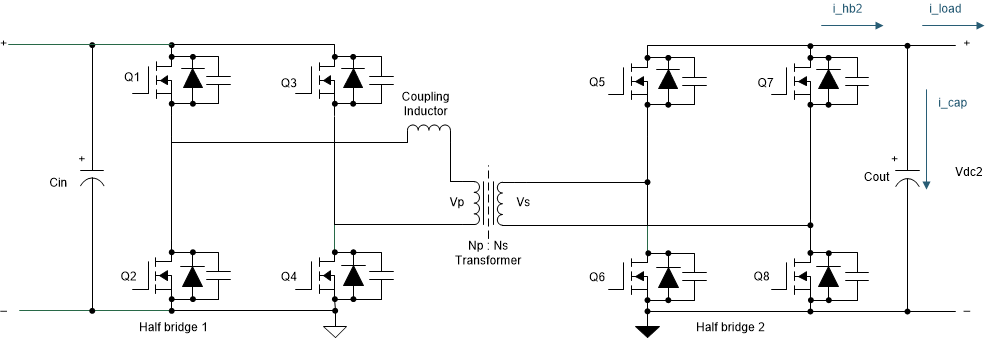
TIDA-010054 Output Current in Dual-Active
                    Bridge Figure 2-19 Output Current in Dual-Active Bridge
TIDA-010054 Output Capacitor
                    Current Figure 2-20 Output Capacitor Current

The capacitor also needs to be able to handle the RMS current, which is calculated with Equation 19.

Equation 19. I C , R M S = φ 2 × π × 1 3 × ( i C 2 2 + i C 2 × i C 3 + i C 3 2 ) + ( 1 - φ 2 × π ) × 1 3 × ( i C 1 2 + i C 1 × i C 2 + i C 2 2 )

where

i C 1 = ( i 1 × N ) - I o u t  
i C 2 = ( i 2 × N ) - I o u t
i C 3 = ( - i 1 × N ) - I o u t