TIDUES6 August 2020 – MONTH
- Description
- Resources
- Features
- Applications
- 5
- 1System Description
- 2System Overview
- 3Hardware, Software, Testing Requirements, and Test Results
- 4Design Files
- 5Software Files
- 6Related Documentation
- 7Terminology
2.4.4.3 Buffer Amplifier Stability for Very-Large Capacitive Loads
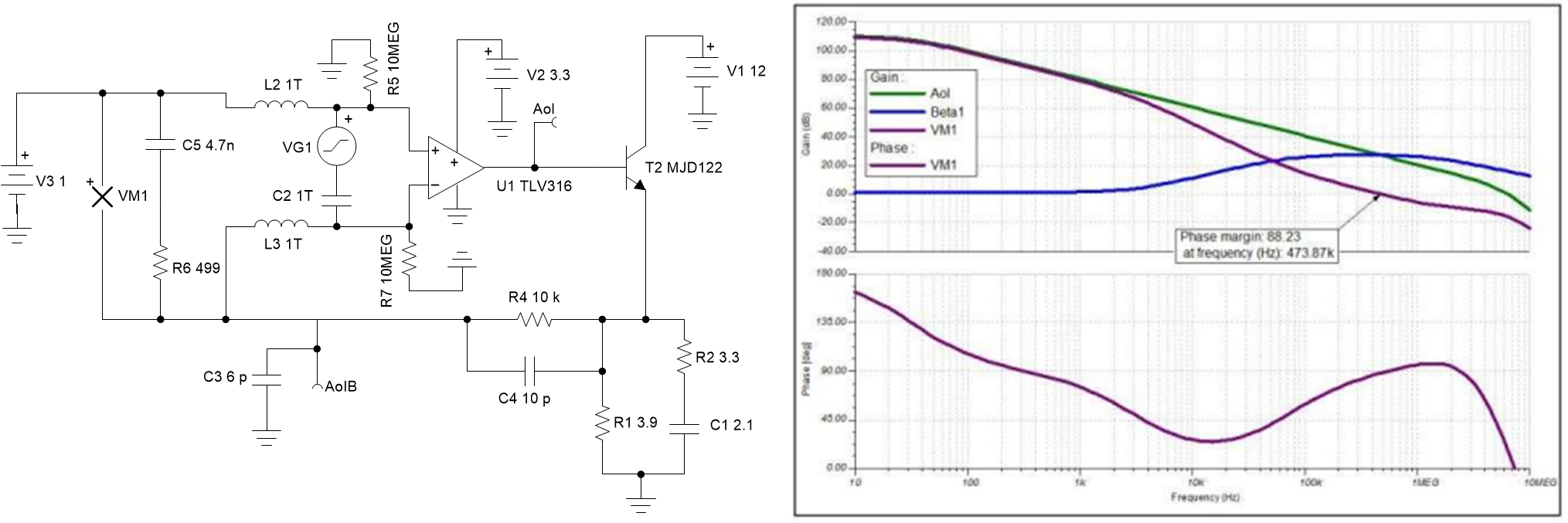
Due to the size of the capacitive load, stability of the buffer amplifier is a concern. Designers can improve capacitive load stability through the use of both noise gain and capacitive feedback compensation. Using rate of closure analysis provides a guideline on the expected phase margin on an amplifier based on the angle of the slopes between the modified open loop gain and 1/β bode plots. A key rule is to ensure the rate of closure is not greater than 20 dB/decade, which ensures the phase margin of the design is greater than 45°. For more information on op amps and stability, see the training resource TI Precision Labs - Ops Amps: Stability 2.
The noise gain compensation consists of implementing high-frequency gain to allow the 1/β of the amplifier to be larger than the modified open-loop gain at the pole introduced by the capacitive load, which allows the rate of the closure to be 20 dB/decade rather than 40 dB/decade. This method retains the desired 0-dB gain at DC that allows the amplifier to continue to operate as a buffer. The noise gain provides the necessary bump in the phase margin to maintain stability across the entire bandwidth of the amplifier and prevent ringing.
This high-frequency gain is implemented with R1, R3, and C6, which creates a zero and provides a 20-dB/decade slope on the 1/β plot above approximately 1 kHz. The rate of closure at the intersection is then |–40 dB/decade + 20 dB/decade| = 20 dB/decade.
To add to the stability improvements found with noise gain, an additional capacitor C1 is used to implement a capacitive feedback, or Cf, compensation. This additional high-frequency pole boosts the phase even more in the area of concern.
Figure 2-11 shows a TINA simulation of the bode plot without the noise gain implemented and Figure 2-12 shows the result of the noise gain.
 Figure 2-11 TINA-TI™ Stability Analysis of EC Mirror Driver Without Compensation
 Figure 2-12 TINA-TI™ Stability Analysis of EC Mirror Driver With Compensation