TIDUET0A November 2019 – July 2020
2.4 System Design Theory
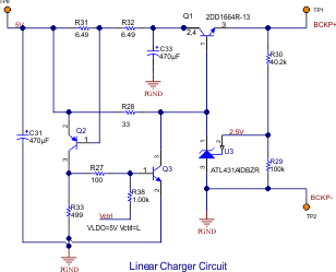
Figure 2-2 shows the linear charger circuit of TIDA-050031. The benefits of the linear charger are simplicity and low cost. Transistors Q2 and Q3 are added to limit the initial charge current and makes the charging current a constant value. The exists of Q2 and Q3 can also avoid Q1 being damaged in a short-circuit condition.
 Figure 2-2 Linear Charger Circuit
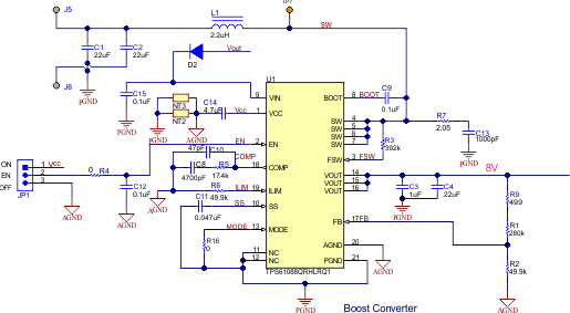
Figure 2-3 shows the TPS61088-Q1 boost converter of TIDA-050031, which is the main circuit of TIDA-050031. The Vin pin of TPS61088-Q1 is supplied by the output voltage through a diode. When the main battery is available, the buck converter is working, Vout is around 8.7 V, so the Vin pin voltage is around 8.4 V considering the forward voltage drop of D2. The EN pin is pulled high to Vcc. So once the main battery is available and the buck converter starts working, the TPS61088-Q1 is enabled at the same time. In this condition, the operating quiescent current at the Vin pin is less then 3uA, and this quiescent is drawn from the Vout instead of the backup battery. So the backup battery lifetime can be greatly prolonged in this configuration.
 Figure 2-3 TPS61088-Q1 Boost Converter
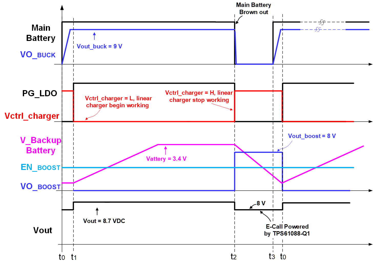
Figure 2-4 shows the operation sequence of TIDA-050031. At time t0, main battery ready. Buck converter starts working. At time t1, LDO output 5V, the PG pin of the LDO gets high, linear charger begin working, it charges the backup battery with a 100mA constant current. At time t2, the main battery browns out, linear charger stops working, the ECall system is powered by the backup battery though the TPS61088-Q1 boost converter. At time t3, the main battery recovery, it supply the ECall system through the buck converter again.
 Figure 2-4 Operation Sequence