TIDUET7G September 2019 – October 2023
- 1
- Description
- Resources
- Features
- Applications
- 6
- 1System Description
-
2System Overview
- 2.1 Block Diagram
- 2.2 Design Considerations
- 2.3
Highlighted Products
- 2.3.1 LMG3422R050 — 600-V GaN With Integrated Driver and Protection
- 2.3.2 TMCS1100 — Precision Isolated Current Sense Monitor
- 2.3.3 UCC27524 — Dual, 5-A, High-Speed Low-Side Power MOSFET Driver
- 2.3.4 UCC27714 — 620-V, 1.8-A, 2.8-A High-Side Low-Side Gate Driver
- 2.3.5 ISO7721 — High Speed, Robust EMC, Reinforced and Basic Dual-Channel Digital Isolator
- 2.3.6 ISO7740 and ISO7720 — High-Speed, Low-Power, Robust EMC Digital Isolators
- 2.3.7 OPA237 — Single-Supply Operational Amplifier
- 2.3.8 INAx180 — Low- and High-Side Voltage Output, Current-Sense Amplifiers
- 2.3.9 TPS560430 — SIMPLE SWITCHER 4-V to 36-V, 600-mA Synchronous Step-Down Converter
- 2.3.10 TLV713 — 150-mA Low-Dropout (LDO) Regulator With Foldback Current Limit for Portable Devices
- 2.3.11 TMP61 — Small Silicon-Based Linear Thermistor for Temperature Sensing
- 2.3.12 CSD18510Q5B — 40-V, N-Channel NexFET MOSFET, Single SON5x6, 0.96 mOhm
- 2.3.13 UCC28911 — 700-V Flyback Switcher With Constant-Voltage, Constant-Current, and Primary-Side Regulation
- 2.3.14 SN74LVC1G3157DRYR — Single-Pole Double-Throw Analog Switch
- 2.4
System Design Theory
- 2.4.1 Totem Pole PFC Stage Design
- 2.4.2
Design Parameters of the LLC Stage
- 2.4.2.1 Determining LLC Transformer Turns Ratio N
- 2.4.2.2 Determining Mg_min and Mg_max
- 2.4.2.3 Determining Equivalent Load Resistance (Re) of Resonant Network
- 2.4.2.4 Selecting Lm and Lr Ratio (Ln) and Qe
- 2.4.2.5 Determining Primary-Side Currents
- 2.4.2.6 Determining Secondary-Side Currents
- 2.4.2.7 Primary-Side GaN and Driver
- 2.4.2.8 Secondary-Side Synchronous MOSFETs
- 2.4.2.9 Output Current Sensing
- 2.4.3 Communication Between the Primary Side and the Secondary Side
-
3Hardware, Software, Testing Requirements, and Test Results
- 3.1
Required Hardware and Software
- 3.1.1 Hardware
- 3.1.2
PFC Stage Software
- 3.1.2.1 Opening Project Inside CCS
- 3.1.2.2 Project Structure
- 3.1.2.3 Using CLA on C2000 MCU to Alleviate CPU Burden
- 3.1.2.4 CPU Utilization and Memory Allocation
- 3.1.2.5 Running the Project
- 3.1.3 LLC Stage Software
- 3.1.4 PFC + LLC Stage Dual Test
- 3.1.5 Live Firmware Update Overview
- 3.2 Testing and Results
- 3.1
Required Hardware and Software
- 4Design Files
- 5Software Files
- 6Related Documentation
- 7About the Author
- 8Revision History
- 132
3.1.5.5 Running the LFU Demonstration With Control Loop Running on the CLA and Test Results
With both flash banks of the device programmed with the custom bootloader and Application images, the LFU demonstration is now ready to run in Standalone mode.
To confirm successful switchover, a variety of different signals, registers and LEDs on the device can be observed.
Apply power to the board. At this point, verify that LED2 (GPIO34 – D2) is OFF and LED1 (GPIO31 -D1) is ON. This indicates that the Bank0 application is the active application being run. If both LEDs (D1 and D2) are ON, then Bank1 is the active application. Observe that the PWMs gate driver signals are not visible on an oscilloscope. This is due to the software waiting for the SCI autobaud lock command from the Microsoft® Windows® PC.
To enable SCI autobaud lock, execute a command from the Microsoft Windows command prompt. This command is similar to the command previously entered when programming bootloader and application. An example command follows:
serial_flash_programmer_appln.exe -d f28003x -k
                        f28003x_fw_upgrade_example\flash_kernel_ex3_sci_flash_kernel_bank0.txt -a
                        f28003x_fw_upgrade_example\llc_f28003x_BANK1FLASH.txt -b 9600 -p
                        COM5

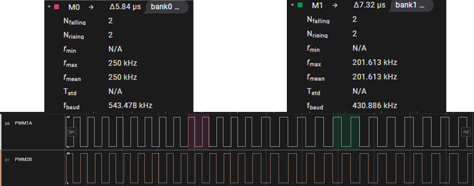
Figure 3-38 Switching Frequency Change Pre- and Post-LFU Operations
Now observe on the controlCARD that the LED1 toggles, thus confirming the execution of the LLC_HAL_toggleLED () function in the background task B1 in llc_main.c. LED2 is OFF if Bank0 has the active application and ON if Bank1 has the active application.
The command prompt window shows the same option flash programming options as previously shown. The device is now ready to switch to the other flash bank. To switch execution to the other bank, Enter “8 – Live DFU” – this programs the new firmware to the inactive bank. When complete, Enter “0 – Done” to complete the process. During downloading to Flash, LED1 stops toggling because background tasks are halted.
After programming the new image to the device, LED2 and LED1 switch from ON to OFF (Bank 1 -> Bank 0) or from OFF to ON (Bank0 -> Bank1). This indication of execution of the new image.
The PWM signal waveforms should now be updated with the new targeted switching frequency (200 kHz) as shown in green (M1), see Figure 3-38.
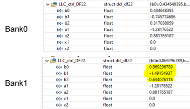
Another step that can be confirmed is the programming of new coefficient for the DF22 controller, this can be done by loading the symbols of Bank0 application into CCS prior to LFU and looking at the contents of the LLC_ctrl_DF22 structure. Specifically observing the targeted control loop parameters b0, b1, and b2. Once the LFU is complete, the symbols for the Bank1 application can be loaded into CCS and the targeted parameters can observed to confirm the switchover and execution of the new image and the appropriate settings. Figure 3-39 illustrates the coefficient values prior and post LFU.

Figure 3-39 Control Loop Parameter Changes Between Different Images on Bank0 vs Bank1