TIDUET7G September 2019 – October 2023
- 1
- Description
- Resources
- Features
- Applications
- 6
- 1System Description
-
2System Overview
- 2.1 Block Diagram
- 2.2 Design Considerations
- 2.3
Highlighted Products
- 2.3.1 LMG3422R050 — 600-V GaN With Integrated Driver and Protection
- 2.3.2 TMCS1100 — Precision Isolated Current Sense Monitor
- 2.3.3 UCC27524 — Dual, 5-A, High-Speed Low-Side Power MOSFET Driver
- 2.3.4 UCC27714 — 620-V, 1.8-A, 2.8-A High-Side Low-Side Gate Driver
- 2.3.5 ISO7721 — High Speed, Robust EMC, Reinforced and Basic Dual-Channel Digital Isolator
- 2.3.6 ISO7740 and ISO7720 — High-Speed, Low-Power, Robust EMC Digital Isolators
- 2.3.7 OPA237 — Single-Supply Operational Amplifier
- 2.3.8 INAx180 — Low- and High-Side Voltage Output, Current-Sense Amplifiers
- 2.3.9 TPS560430 — SIMPLE SWITCHER 4-V to 36-V, 600-mA Synchronous Step-Down Converter
- 2.3.10 TLV713 — 150-mA Low-Dropout (LDO) Regulator With Foldback Current Limit for Portable Devices
- 2.3.11 TMP61 — Small Silicon-Based Linear Thermistor for Temperature Sensing
- 2.3.12 CSD18510Q5B — 40-V, N-Channel NexFET MOSFET, Single SON5x6, 0.96 mOhm
- 2.3.13 UCC28911 — 700-V Flyback Switcher With Constant-Voltage, Constant-Current, and Primary-Side Regulation
- 2.3.14 SN74LVC1G3157DRYR — Single-Pole Double-Throw Analog Switch
- 2.4
System Design Theory
- 2.4.1 Totem Pole PFC Stage Design
- 2.4.2
Design Parameters of the LLC Stage
- 2.4.2.1 Determining LLC Transformer Turns Ratio N
- 2.4.2.2 Determining Mg_min and Mg_max
- 2.4.2.3 Determining Equivalent Load Resistance (Re) of Resonant Network
- 2.4.2.4 Selecting Lm and Lr Ratio (Ln) and Qe
- 2.4.2.5 Determining Primary-Side Currents
- 2.4.2.6 Determining Secondary-Side Currents
- 2.4.2.7 Primary-Side GaN and Driver
- 2.4.2.8 Secondary-Side Synchronous MOSFETs
- 2.4.2.9 Output Current Sensing
- 2.4.3 Communication Between the Primary Side and the Secondary Side
-
3Hardware, Software, Testing Requirements, and Test Results
- 3.1
Required Hardware and Software
- 3.1.1 Hardware
- 3.1.2
PFC Stage Software
- 3.1.2.1 Opening Project Inside CCS
- 3.1.2.2 Project Structure
- 3.1.2.3 Using CLA on C2000 MCU to Alleviate CPU Burden
- 3.1.2.4 CPU Utilization and Memory Allocation
- 3.1.2.5 Running the Project
- 3.1.3 LLC Stage Software
- 3.1.4 PFC + LLC Stage Dual Test
- 3.1.5 Live Firmware Update Overview
- 3.2 Testing and Results
- 3.1
Required Hardware and Software
- 4Design Files
- 5Software Files
- 6Related Documentation
- 7About the Author
- 8Revision History
- 132
3.1.2.5.2.3 Running Code
- The project is programmed to drive the inrush relay and clear the trip after a set amount of time, that is, autoStartSlew==100. The software is programmed to do so in this lab. An input voltage must be applied after selecting run and before this autoslew counter reaches 100. If the counter reaches 100, before voltage is applied at the input, the code must be reset. For which the controller must be brought out of real time mode, a reset performed and restarted. Repeat steps from 3.
- Now run the project by clicking
 .
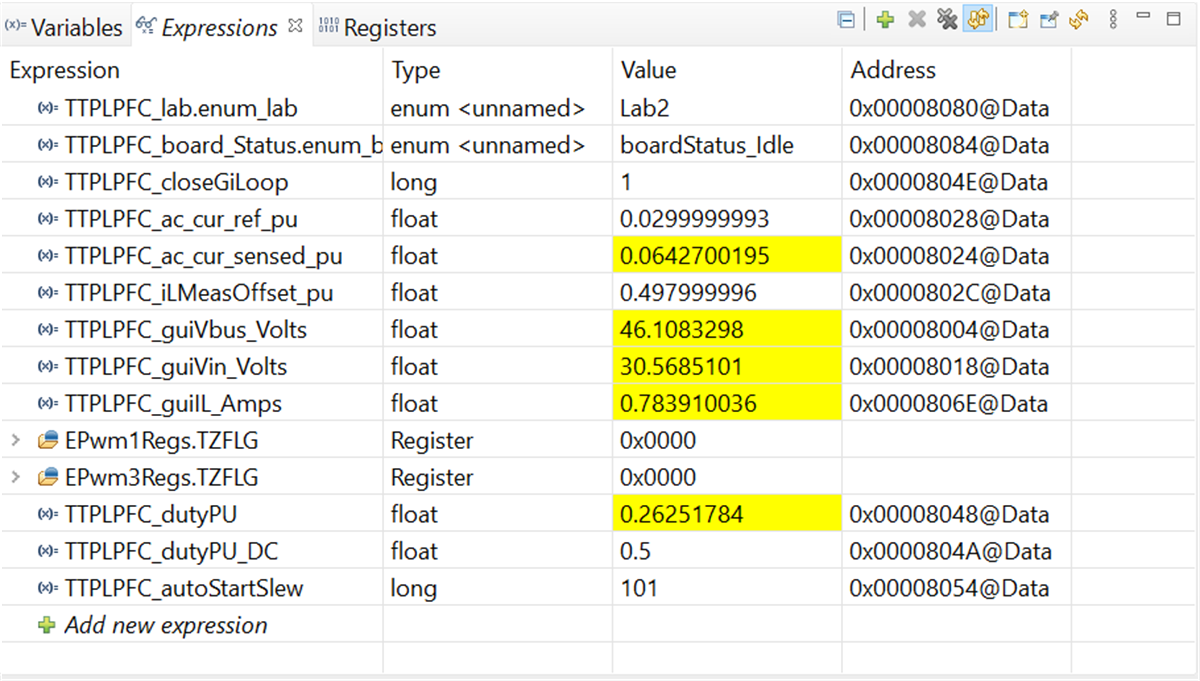
. - Apply an input voltage of approximately 30 V before the TTPLPFC_autoStartSlew reaches 100. As soon TTPLPFC_autoStartSlew reaches 100, the inrush relay is triggered, and PWM trip is cleared along with closing the current loop flag.
 Figure 3-12 PFC Lab 2: Watch Expression, After Closed Current Loop Operation Begins
 - The input current regulates around 0.7 A, and the output voltage boosts to approximately 46 V.
- This action verifies the current compensator design.
- To bring the system to a safe stop, bring the input DC voltage down to zero, observe the TTPLPFC_guiVBus_Volts comes down to zero as well.
Fully halting the MCU when in real-time mode is a two-step process. First halt the processor by using the Halt button on the toolbar (
 ) or by using Target → Halt. Then take the MCU out of real-time mode by clicking on
  . Finally, reset the MCU by clicking on
  .
. - Close CCS debug session by clicking on Terminate Debug Session (Target→Terminate all)
 .
.