TIDUET7G September   2019  – October 2023


  1.   1
  2.   Description
  3.   Resources
  4.   Features
  5.   Applications
  6.   6
  7. 1System Description
    1. 1.1 Key System Specifications
  8. 2System Overview
    1. 2.1 Block Diagram
    2. 2.2 Design Considerations
    3. 2.3 Highlighted Products
      1. 2.3.1  LMG3422R050 — 600-V GaN With Integrated Driver and Protection
      2. 2.3.2  TMCS1100 — Precision Isolated Current Sense Monitor
      3. 2.3.3  UCC27524 — Dual, 5-A, High-Speed Low-Side Power MOSFET Driver
      4. 2.3.4  UCC27714 — 620-V, 1.8-A, 2.8-A High-Side Low-Side Gate Driver
      5. 2.3.5  ISO7721 — High Speed, Robust EMC, Reinforced and Basic Dual-Channel Digital Isolator
      6. 2.3.6  ISO7740 and ISO7720 — High-Speed, Low-Power, Robust EMC Digital Isolators
      7. 2.3.7  OPA237 — Single-Supply Operational Amplifier
      8. 2.3.8  INAx180 — Low- and High-Side Voltage Output, Current-Sense Amplifiers
      9. 2.3.9  TPS560430 — SIMPLE SWITCHER 4-V to 36-V, 600-mA Synchronous Step-Down Converter
      10. 2.3.10 TLV713 — 150-mA Low-Dropout (LDO) Regulator With Foldback Current Limit for Portable Devices
      11. 2.3.11 TMP61 — Small Silicon-Based Linear Thermistor for Temperature Sensing
      12. 2.3.12 CSD18510Q5B — 40-V, N-Channel NexFET MOSFET, Single SON5x6, 0.96 mOhm
      13. 2.3.13 UCC28911 — 700-V Flyback Switcher With Constant-Voltage, Constant-Current, and Primary-Side Regulation
      14. 2.3.14 SN74LVC1G3157DRYR — Single-Pole Double-Throw Analog Switch
    4. 2.4 System Design Theory
      1. 2.4.1 Totem Pole PFC Stage Design
        1. 2.4.1.1 Design Parameters of the PFC Stage
        2. 2.4.1.2 Current Calculations
        3. 2.4.1.3 PFC Boost Inductor
        4. 2.4.1.4 Output Capacitor
        5. 2.4.1.5 Fast and Slow Switches
        6. 2.4.1.6 AC Current Sensing Circuits
        7. 2.4.1.7 Temperature Sensing
      2. 2.4.2 Design Parameters of the LLC Stage
        1. 2.4.2.1 Determining LLC Transformer Turns Ratio N
        2. 2.4.2.2 Determining Mg_min and Mg_max
        3. 2.4.2.3 Determining Equivalent Load Resistance (Re) of Resonant Network
        4. 2.4.2.4 Selecting Lm and Lr Ratio (Ln) and Qe
        5. 2.4.2.5 Determining Primary-Side Currents
        6. 2.4.2.6 Determining Secondary-Side Currents
        7. 2.4.2.7 Primary-Side GaN and Driver
        8. 2.4.2.8 Secondary-Side Synchronous MOSFETs
        9. 2.4.2.9 Output Current Sensing
      3. 2.4.3 Communication Between the Primary Side and the Secondary Side
  9. 3Hardware, Software, Testing Requirements, and Test Results
    1. 3.1 Required Hardware and Software
      1. 3.1.1 Hardware
        1. 3.1.1.1 Test Conditions
        2. 3.1.1.2 Test Equipment Required for Board Validation
        3. 3.1.1.3 Test Procedure
          1. 3.1.1.3.1 System Test: Dual Stages
          2. 3.1.1.3.2 PFC Stage Test
          3. 3.1.1.3.3 LLC Stage Test
      2. 3.1.2 PFC Stage Software
        1. 3.1.2.1 Opening Project Inside CCS
        2. 3.1.2.2 Project Structure
        3. 3.1.2.3 Using CLA on C2000 MCU to Alleviate CPU Burden
        4. 3.1.2.4 CPU Utilization and Memory Allocation
        5. 3.1.2.5 Running the Project
          1. 3.1.2.5.1 Lab 1: Open Loop, DC (PFC Mode)
            1. 3.1.2.5.1.1 Setting Software Options for Lab 1
            2. 3.1.2.5.1.2 Building and Loading Project
            3. 3.1.2.5.1.3 Setup Debug Environment Windows
            4. 3.1.2.5.1.4 Using Real-Time Emulation
            5. 3.1.2.5.1.5 Running Code
          2. 3.1.2.5.2 Lab 2: Closed Current Loop DC
            1. 3.1.2.5.2.1 Setting Software Options for Lab 2
            2. 3.1.2.5.2.2 Building and Loading Project and Setting up Debug
            3. 3.1.2.5.2.3 Running Code
          3. 3.1.2.5.3 Lab 3: Closed Current Loop, AC (PFC)
            1. 3.1.2.5.3.1 Setting Software Options for Lab 3
            2. 3.1.2.5.3.2 Building and Loading Project and Setting up Debug
            3. 3.1.2.5.3.3 Running Code
          4. 3.1.2.5.4 Lab 4: Closed Voltage and Current Loop (PFC)
            1. 3.1.2.5.4.1 Setting Software Options for Lab 4
            2. 3.1.2.5.4.2 Building and Loading Project and Setting up Debug
            3. 3.1.2.5.4.3 Running Code
      3. 3.1.3 LLC Stage Software
        1. 3.1.3.1 Opening Project Inside CCS
        2. 3.1.3.2 Project Structure
        3. 3.1.3.3 Software Flow
        4. 3.1.3.4 CPU Utilization and Memory Allocation
        5. 3.1.3.5 Running the Project
          1. 3.1.3.5.1 Lab 1: Open-Loop Control
            1. 3.1.3.5.1.1 Software Setup
            2. 3.1.3.5.1.2 Build and Load the Project
            3. 3.1.3.5.1.3 Debug Environment Windows
            4. 3.1.3.5.1.4 Run the Code
          2. 3.1.3.5.2 Lab 2: Closed-Loop Control With SFRA
            1. 3.1.3.5.2.1 Software Setup
            2. 3.1.3.5.2.2 Build and Load the Project
            3. 3.1.3.5.2.3 Debug Environment Windows
            4. 3.1.3.5.2.4 Run the Code
      4. 3.1.4 PFC + LLC Stage Dual Test
        1. 3.1.4.1 Hardware Setup
        2. 3.1.4.2 System Test Procedure
        3. 3.1.4.3 FSI Software in TIDA-010062
      5. 3.1.5 Live Firmware Update Overview
        1. 3.1.5.1 Live Firmware Update Description
        2. 3.1.5.2 Software Structure
        3. 3.1.5.3 LFU on LLC Stage Software
          1. 3.1.5.3.1 Opening Project Inside CCS
        4. 3.1.5.4 Loading the Custom Bootloader and Application to Flash Using CCS
        5. 3.1.5.5 Running the LFU Demonstration With Control Loop Running on the CLA and Test Results
    2. 3.2 Testing and Results
      1. 3.2.1 Performance, Data, and Curve
        1. 3.2.1.1 Efficiency, iTHD, and PF of the PFC Stage
        2. 3.2.1.2 Efficiency of the LLC Stage
        3. 3.2.1.3 Efficiency of the Whole System
      2. 3.2.2 Functional Waveforms
        1. 3.2.2.1 Start-up
        2. 3.2.2.2 Hall Sensor
        3. 3.2.2.3 PFC Working Waveforms
        4. 3.2.2.4 LLC Working Waveforms
  10. 4Design Files
    1. 4.1 Schematics
    2. 4.2 Bill of Materials
    3. 4.3 PCB Layout Recommendations
      1. 4.3.1 Power Stage Specific Guidelines
      2. 4.3.2 Gate Driver Specific Guidelines
      3. 4.3.3 Layout Prints
    4. 4.4 Altium Project
    5. 4.5 Gerber Files
    6. 4.6 Assembly Drawings
  11. 5Software Files
  12. 6Related Documentation
    1. 6.1 Trademarks
  13. 7About the Author
  14. 8Revision History
  15.   132

Start-up

Figure 3-45 shows the no-load, start-up waveform. Figure 3-46 shows the half-load, start-up waveform.
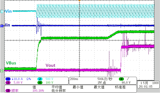
GUID-5B89725D-7C46-4F95-90CF-27117EB9EBE2-low.pngFigure 3-45 System Start-up With No Load
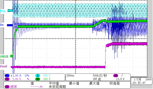
GUID-670B1AEF-DD10-4BE3-8655-E073FA648B07-low.pngFigure 3-46 System Start-up With 50% Load