TIDUET7G September 2019 – October 2023
- 1
- Description
- Resources
- Features
- Applications
- 6
- 1System Description
-
2System Overview
- 2.1 Block Diagram
- 2.2 Design Considerations
- 2.3
Highlighted Products
- 2.3.1 LMG3422R050 — 600-V GaN With Integrated Driver and Protection
- 2.3.2 TMCS1100 — Precision Isolated Current Sense Monitor
- 2.3.3 UCC27524 — Dual, 5-A, High-Speed Low-Side Power MOSFET Driver
- 2.3.4 UCC27714 — 620-V, 1.8-A, 2.8-A High-Side Low-Side Gate Driver
- 2.3.5 ISO7721 — High Speed, Robust EMC, Reinforced and Basic Dual-Channel Digital Isolator
- 2.3.6 ISO7740 and ISO7720 — High-Speed, Low-Power, Robust EMC Digital Isolators
- 2.3.7 OPA237 — Single-Supply Operational Amplifier
- 2.3.8 INAx180 — Low- and High-Side Voltage Output, Current-Sense Amplifiers
- 2.3.9 TPS560430 — SIMPLE SWITCHER 4-V to 36-V, 600-mA Synchronous Step-Down Converter
- 2.3.10 TLV713 — 150-mA Low-Dropout (LDO) Regulator With Foldback Current Limit for Portable Devices
- 2.3.11 TMP61 — Small Silicon-Based Linear Thermistor for Temperature Sensing
- 2.3.12 CSD18510Q5B — 40-V, N-Channel NexFET MOSFET, Single SON5x6, 0.96 mOhm
- 2.3.13 UCC28911 — 700-V Flyback Switcher With Constant-Voltage, Constant-Current, and Primary-Side Regulation
- 2.3.14 SN74LVC1G3157DRYR — Single-Pole Double-Throw Analog Switch
- 2.4
System Design Theory
- 2.4.1 Totem Pole PFC Stage Design
- 2.4.2
Design Parameters of the LLC Stage
- 2.4.2.1 Determining LLC Transformer Turns Ratio N
- 2.4.2.2 Determining Mg_min and Mg_max
- 2.4.2.3 Determining Equivalent Load Resistance (Re) of Resonant Network
- 2.4.2.4 Selecting Lm and Lr Ratio (Ln) and Qe
- 2.4.2.5 Determining Primary-Side Currents
- 2.4.2.6 Determining Secondary-Side Currents
- 2.4.2.7 Primary-Side GaN and Driver
- 2.4.2.8 Secondary-Side Synchronous MOSFETs
- 2.4.2.9 Output Current Sensing
- 2.4.3 Communication Between the Primary Side and the Secondary Side
-
3Hardware, Software, Testing Requirements, and Test Results
- 3.1
Required Hardware and Software
- 3.1.1 Hardware
- 3.1.2
PFC Stage Software
- 3.1.2.1 Opening Project Inside CCS
- 3.1.2.2 Project Structure
- 3.1.2.3 Using CLA on C2000 MCU to Alleviate CPU Burden
- 3.1.2.4 CPU Utilization and Memory Allocation
- 3.1.2.5 Running the Project
- 3.1.3 LLC Stage Software
- 3.1.4 PFC + LLC Stage Dual Test
- 3.1.5 Live Firmware Update Overview
- 3.2 Testing and Results
- 3.1
Required Hardware and Software
- 4Design Files
- 5Software Files
- 6Related Documentation
- 7About the Author
- 8Revision History
- 132
3.1.1.1 Test Conditions
For input, the power supply source (VIN) must range from 100-V to 265-V AC. Set the input current limit of the input AC source to 15 A. For output, use an electronic variable load or a variable resistive load, which must be rated for ≥ 15 V and must vary the load current from 0 A to 90 A.
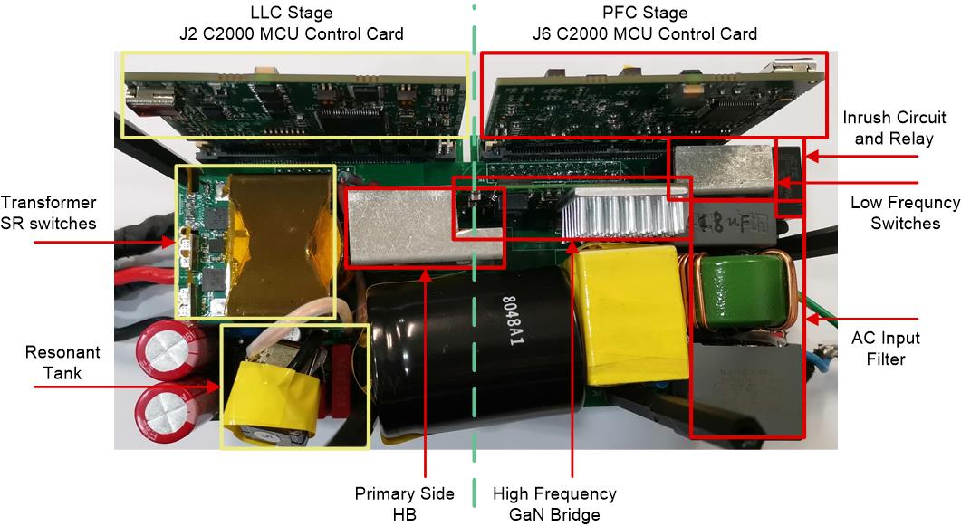
This section details the hardware and the different sections on the board. If only using the firmware of the design through powerSUITE, this section might not be valid. The key resources used for controlling the PFC stage on the MCU are listed in Table 3-1. The key resources used for controlling the LLC stage on the MCU are listed in Table 3-2. Figure 3-1 shows the key power stage and connectors on the design board.
 Figure 3-1 Board Overview
| SIGNAL NAME | HSEC PIN NUMBER | FUNCTION |
|---|---|---|
| PWM-1A | 49 | PWM: low-frequency MOSFET leg, high-side switch |
| PWM-1B | 51 | PWM: low-frequency MOSFET leg, low-side switch |
| PWM-3A | 50 | PWM: high-frequency GaN leg, high-side switch. |
| PWM-3B | 52 | PWM: high-frequency GaN leg, low-side switch. |
| Iac | 18 | ADC with CMPSS: AC return current measurement |
| VL | 20 | ADC: AC voltage line |
| VN | 17 | ADC: AC voltage neutral |
| Vbus | 24 | ADC: bus voltage |
| In Rush Relay | 67 | GPIO: used to control the inrush relay |
| GaN Fault | 56 | GPIO: GaN fault signal |
| AC Current Sense GainChange | 63 | GPIO: controls the gain stage |
| SIGNAL NAME | HSEC PIN NUMBER | FUNCTION |
|---|---|---|
| PWM-1A | 49 | High-side drive signal for primary side HB |
| PWM-1B | 51 | Low-side drive signal for primary side HB |
| PWM-2A | 53 | Drive signal for SRA |
| PWM-2B | 55 | Drive signal for SRB |
| VOUT | 25 | ADC with CMPSS: Output voltage measurement |
| IOUT | 15 | ADC with CMPSS: Resonant current measurement |
| Ireso | 21 | ADC with CMPSS: Output current measurement |