TIDUET7G September 2019 – October 2023
- 1
- Description
- Resources
- Features
- Applications
- 6
- 1System Description
-
2System Overview
- 2.1 Block Diagram
- 2.2 Design Considerations
- 2.3
Highlighted Products
- 2.3.1 LMG3422R050 — 600-V GaN With Integrated Driver and Protection
- 2.3.2 TMCS1100 — Precision Isolated Current Sense Monitor
- 2.3.3 UCC27524 — Dual, 5-A, High-Speed Low-Side Power MOSFET Driver
- 2.3.4 UCC27714 — 620-V, 1.8-A, 2.8-A High-Side Low-Side Gate Driver
- 2.3.5 ISO7721 — High Speed, Robust EMC, Reinforced and Basic Dual-Channel Digital Isolator
- 2.3.6 ISO7740 and ISO7720 — High-Speed, Low-Power, Robust EMC Digital Isolators
- 2.3.7 OPA237 — Single-Supply Operational Amplifier
- 2.3.8 INAx180 — Low- and High-Side Voltage Output, Current-Sense Amplifiers
- 2.3.9 TPS560430 — SIMPLE SWITCHER 4-V to 36-V, 600-mA Synchronous Step-Down Converter
- 2.3.10 TLV713 — 150-mA Low-Dropout (LDO) Regulator With Foldback Current Limit for Portable Devices
- 2.3.11 TMP61 — Small Silicon-Based Linear Thermistor for Temperature Sensing
- 2.3.12 CSD18510Q5B — 40-V, N-Channel NexFET MOSFET, Single SON5x6, 0.96 mOhm
- 2.3.13 UCC28911 — 700-V Flyback Switcher With Constant-Voltage, Constant-Current, and Primary-Side Regulation
- 2.3.14 SN74LVC1G3157DRYR — Single-Pole Double-Throw Analog Switch
- 2.4
System Design Theory
- 2.4.1 Totem Pole PFC Stage Design
- 2.4.2
Design Parameters of the LLC Stage
- 2.4.2.1 Determining LLC Transformer Turns Ratio N
- 2.4.2.2 Determining Mg_min and Mg_max
- 2.4.2.3 Determining Equivalent Load Resistance (Re) of Resonant Network
- 2.4.2.4 Selecting Lm and Lr Ratio (Ln) and Qe
- 2.4.2.5 Determining Primary-Side Currents
- 2.4.2.6 Determining Secondary-Side Currents
- 2.4.2.7 Primary-Side GaN and Driver
- 2.4.2.8 Secondary-Side Synchronous MOSFETs
- 2.4.2.9 Output Current Sensing
- 2.4.3 Communication Between the Primary Side and the Secondary Side
-
3Hardware, Software, Testing Requirements, and Test Results
- 3.1
Required Hardware and Software
- 3.1.1 Hardware
- 3.1.2
PFC Stage Software
- 3.1.2.1 Opening Project Inside CCS
- 3.1.2.2 Project Structure
- 3.1.2.3 Using CLA on C2000 MCU to Alleviate CPU Burden
- 3.1.2.4 CPU Utilization and Memory Allocation
- 3.1.2.5 Running the Project
- 3.1.3 LLC Stage Software
- 3.1.4 PFC + LLC Stage Dual Test
- 3.1.5 Live Firmware Update Overview
- 3.2 Testing and Results
- 3.1
Required Hardware and Software
- 4Design Files
- 5Software Files
- 6Related Documentation
- 7About the Author
- 8Revision History
- 132
3.1.5.3.1 Opening Project Inside CCS
Use the following steps to start the project in CCS:
- Install CCS from the Code Composer Studio (CCS) Integrated Development Environment (IDE) tools folder, CCSV12.0 or above is recommended
- Install C2000Ware DigitalPower SDK at the C2000Ware Digital Power SDK tools
folder. Note: powerSUITE is installed with the SDK in the default install.
- Go to View → Resource Explorer. Under the TI Resource Explorer, go to C2000Ware DigitalPower SDK. To open the reference design software as it is (opens firmware as it was run on this design and hardware, requires the board to be exactly the same as this reference design)
- Under C2000Ware DigitalPower SDK, select Development Kits → CCM Totem Pole PFC TIDA-010062, and click on Run <Import> Project
- These steps import the project, and the development kit or designs page shows up. This page can be used to browse all the information on the design including this user guide, test reports, hardware design files, and so forth.
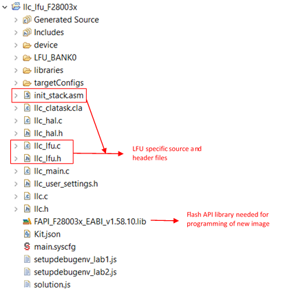
- Click Import F28003x LFU DC-DC Project
- This action imports the project
into the workspace environment, and a main.syscfg page with a GUI similar to
Figure 3-37
appears

Figure 3-37 Typical LFU-Based SystemClick the
main.syscfgfile, a GUI page opens with modifiable options for the PFC design. Use this GUI to change the parameters for an adapted concept, like power rating, inductance, capacitance, sensing circuit parameters, and so forth.For the purposes of LFU, make sure the following options are selected:
- LLC Lab → Closed Loop
- Control On → CLA
- SFRA Enabled → Disabled
- Once the specified settings have been selected. Build the project for each
different build configuration in this order: LFU_BANK0, LFU_BANK1. Note: The project needs to be built in this order since the firmware on Bank1 is built using Bank0 as a reference.
See Section 3.1.3.5 for more information on the specific labs on how to debug them on hardware.