TIDUEW7 May   2020


  1.    Description
  2.    Resources
  3.    Features
  4.    Applications
  5.    Design Images
  6. 1System Description
    1. 1.1 Key System Specifications
  7. 2System Overview
    1. 2.1 Block Diagram
    2. 2.2 Design Considerations
      1. 2.2.1 Processor – i.MX 6ULL Applications Processor
      2. 2.2.2 i.MX 6ULL Memory Interfaces
        1. 2.2.2.1 DDR3L
        2. 2.2.2.2 Quad SPI NOR Flash
        3. 2.2.2.3 eMMC iNAND
        4. 2.2.2.4 SD Card Connector
      3. 2.2.3 USB to UART Converter
      4. 2.2.4 USB Ports
      5. 2.2.5 LCD Screen Connector
      6. 2.2.6 JTAG Header
      7. 2.2.7 USB2ANY Header
      8. 2.2.8 Functional Switches and Status LEDs
      9. 2.2.9 GPIO Expansion Connector
    3. 2.3 Highlighted Products
      1. 2.3.1 TPS6521815 - Power Management IC
      2. 2.3.2 DP83849I - Dual Ethernet PHY
      3. 2.3.3 INA3221 - Current Monitor
      4. 2.3.4 Reset Scheme
      5. 2.3.5 TPS2054B, TPS22964C - Auxiliary Load Switches
    4. 2.4 System Design Theory
      1. 2.4.1 Power Estimation
      2. 2.4.2 Power Sequencing
      3. 2.4.3 I2C Device Chain
      4. 2.4.4 Clock Scheme
      5. 2.4.5 BOOT Configuration
      6. 2.4.6 PCB Floor Planning
  8. 3Getting Started, Testing Setup, and Test Results
    1. 3.1 Getting Started with Hardware and Software
      1. 3.1.1 Hardware
        1. 3.1.1.1 On-board LED Information
      2. 3.1.2 Software
        1. 3.1.2.1 Booting of TIDA-050043
        2. 3.1.2.2 Example Linux Commands for Testing TIDA-050043
  9. 4Design Files
    1. 4.1 Schematics
    2. 4.2 Bill of Materials
    3. 4.3 CAD Files
    4. 4.4 Gerber Files
    5. 4.5 Assembly Drawings
  10. 5Software Files
  11. 6Related Documentation
    1. 6.1 Trademarks
    2. 6.2 Third-Party Products Disclaimer

I2C Device Chain

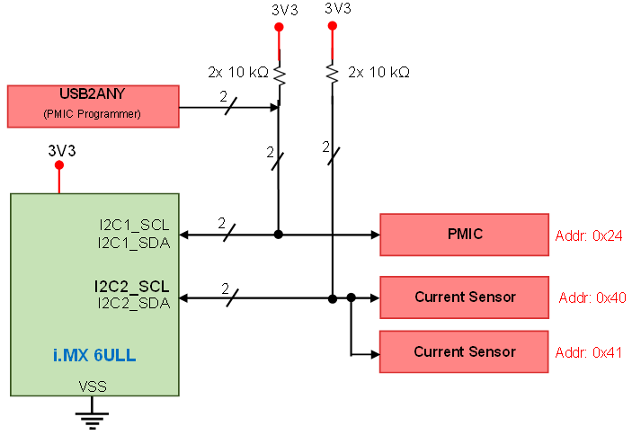
Figure 18 shows the I2C channel mapping from the processor to each slave device.

Figure 18. I2C Device ChainTIDA-050043 tida-050043-i2c-tiduew7.gif