TIDUEW7 May   2020


  1.    Description
  2.    Resources
  3.    Features
  4.    Applications
  5.    Design Images
  6. 1System Description
    1. 1.1 Key System Specifications
  7. 2System Overview
    1. 2.1 Block Diagram
    2. 2.2 Design Considerations
      1. 2.2.1 Processor – i.MX 6ULL Applications Processor
      2. 2.2.2 i.MX 6ULL Memory Interfaces
        1. 2.2.2.1 DDR3L
        2. 2.2.2.2 Quad SPI NOR Flash
        3. 2.2.2.3 eMMC iNAND
        4. 2.2.2.4 SD Card Connector
      3. 2.2.3 USB to UART Converter
      4. 2.2.4 USB Ports
      5. 2.2.5 LCD Screen Connector
      6. 2.2.6 JTAG Header
      7. 2.2.7 USB2ANY Header
      8. 2.2.8 Functional Switches and Status LEDs
      9. 2.2.9 GPIO Expansion Connector
    3. 2.3 Highlighted Products
      1. 2.3.1 TPS6521815 - Power Management IC
      2. 2.3.2 DP83849I - Dual Ethernet PHY
      3. 2.3.3 INA3221 - Current Monitor
      4. 2.3.4 Reset Scheme
      5. 2.3.5 TPS2054B, TPS22964C - Auxiliary Load Switches
    4. 2.4 System Design Theory
      1. 2.4.1 Power Estimation
      2. 2.4.2 Power Sequencing
      3. 2.4.3 I2C Device Chain
      4. 2.4.4 Clock Scheme
      5. 2.4.5 BOOT Configuration
      6. 2.4.6 PCB Floor Planning
  8. 3Getting Started, Testing Setup, and Test Results
    1. 3.1 Getting Started with Hardware and Software
      1. 3.1.1 Hardware
        1. 3.1.1.1 On-board LED Information
      2. 3.1.2 Software
        1. 3.1.2.1 Booting of TIDA-050043
        2. 3.1.2.2 Example Linux Commands for Testing TIDA-050043
  9. 4Design Files
    1. 4.1 Schematics
    2. 4.2 Bill of Materials
    3. 4.3 CAD Files
    4. 4.4 Gerber Files
    5. 4.5 Assembly Drawings
  10. 5Software Files
  11. 6Related Documentation
    1. 6.1 Trademarks
    2. 6.2 Third-Party Products Disclaimer

Reset Scheme

The reset scheme for this project is shown in Figure 14. The DCDC6 low-power buck regulator from TPS6521815 provides the VSNVS voltage from the coin-cell. If the coin-cell is not inserted, the PMIC will still provide VSNVS supply first through SYS_BU input. This is critical to ensure the power-up sequence is correct. When VSNVS is stable along with all the power outputs, the PGOOD pin will de-assert the Power-ON Reset (POR_B).

A reset push-button is connected to the watchdog output of the i.MX 6ULL processor in a wire-OR configuration, which goes into the PB input of a TPS342x push-button controller. The push-button controller can override the enable signal (PWR_EN) to the PMIC and the POR_B input on the processor simultaneously, forcing the system to reset. To shut the system down completely, a separate push-button connected to the ONOFF pin of the processor is used.
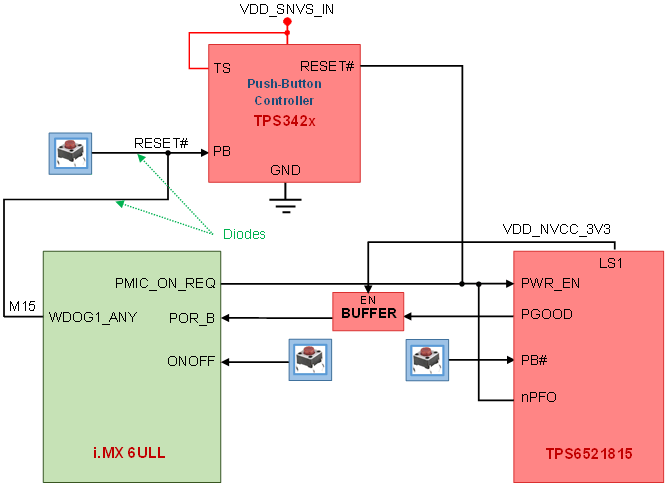
Figure 14. Reset SchemeTIDA-050043 tida-050043-reset-tiduew7.gif