TIDUEW7 May 2020
- Description
- Resources
- Features
- Applications
- Design Images
- 1System Description
-
2System Overview
- 2.1 Block Diagram
- 2.2 Design Considerations
- 2.3 Highlighted Products
- 2.4 System Design Theory
- 3Getting Started, Testing Setup, and Test Results
- 4Design Files
- 5Software Files
- 6Related Documentation
2.3.5 TPS2054B, TPS22964C - Auxiliary Load Switches
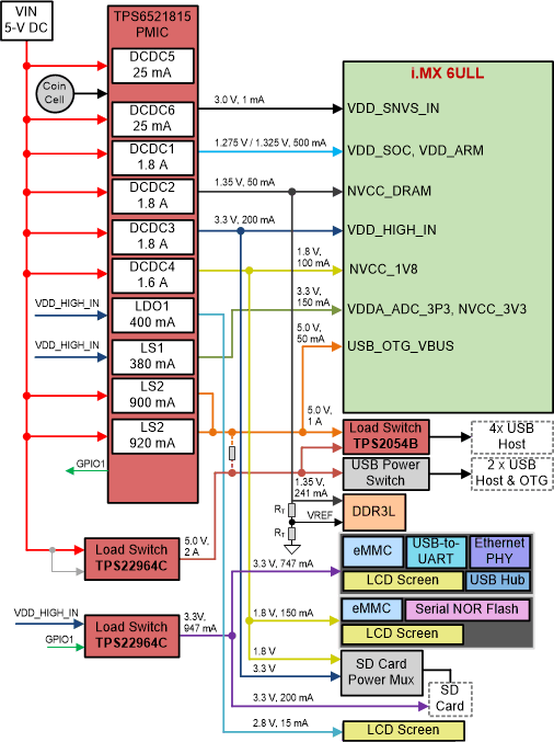
Figure 15 shows the full power architecture. Each peripheral device added to a design may require additional power in addition to what is required by the processor. For this design, we had to add load switches (TPS22964C, TPS2054B) for powering the multiple USB ports and an additional load switch (TPS22964C) for 3.3 V peripherals for the MIPI CSI. Both of these voltages are already available in the design: 5 V is the main input power supply voltage and 3.3 V is generated by DCDC3 of the TPS6521815. As a result, only load switches were added to enable and disable these supply rails, as opposed to adding additional DC-DC or LDO voltage regulators.
Finally, it is sometimes necessary to terminate DDR memory. DDR termination provides a supply (0.675 V) that is half the voltage of the main supply (1.35 V) with the ability to sink or source current. If only one channel of DDR is used, the current consumption is low, or the routing is point-to-point, then tapping off the center of an evenly matched voltage divider may be sufficient. In other cases, a DDR terminator power IC is needed. For this design, we used the matched resistor divider option to terminate the single DDR3L memory IC in the system.
