TIDUEX8 September   2020


  1.   Description
  2.   Resources
  3.   Features
  4.   Applications
  5.   5
  6. 1System Description
    1. 1.1 Key System Specifications
  7. 2System Overview
    1. 2.1 Block Diagram
    2. 2.2 Highlighted Products
      1. 2.2.1 TPS23730
      2. 2.2.2 TLV431
    3. 2.3 System Design Theory
      1. 2.3.1 IEEE802.3bt Introduction
  8. 3Hardware, Testing Requirements, and Test Results
    1. 3.1 Required Hardware
      1. 3.1.1 Hardware
    2. 3.2 Testing and Results
      1. 3.2.1 Test Setup
      2. 3.2.2 Test Results
        1. 3.2.2.1 Efficiency
        2. 3.2.2.2 Control Loop Gain/Stability
        3. 3.2.2.3 Load Transient
        4. 3.2.2.4 Input and Output Ripple
        5. 3.2.2.5 Switching Waveforms
        6. 3.2.2.6 Start Up Response
        7. 3.2.2.7 Soft-Stop Response
        8. 3.2.2.8 Output Short Circuit Response
        9. 3.2.2.9 Thermal Performance
  9. 4Design Files
    1. 4.1 Schematics
    2. 4.2 Bill of Materials
    3. 4.3 PCB Layout Recommendations
      1. 4.3.1 Layout Prints
    4. 4.4 Altium Project
    5. 4.5 Gerber Files
    6. 4.6 Assembly Drawings
  10. 5Related Documentation
    1. 5.1 Trademarks
  11. 6Terminology
  12. 7About the Author

Start Up Response

Figure 3-12 and Figure 3-13 shows the 5-V output start up waveform after the application of 48 V at the PoE input (J1). The output was loaded to 10 A Figure 3-12 and 0 A Figure 3-13. Both waveforms include the output voltage (yellow), VCC (pink), VOUT (blue) and output current (green).
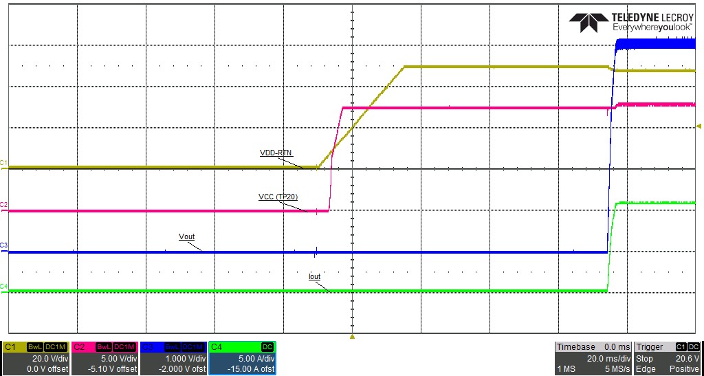
GUID-BAEF45D2-B5A1-4ABC-BE2A-F12414534A4C-low.jpg Figure 3-12 Startup Waveforms at 10-A Load, 20 ms-div
GUID-BA3AD725-B798-4184-9732-C4F9D35CE67D-low.jpg Figure 3-13 Startup Waveforms at 0 A Load, 20 ms-div