TIDUEY7 July 2021
- Description
- Resources
- Features
- Applications
- 5
- 1System Description
-
2System Overview
- 2.1 Block Diagram
- 2.2
Design Considerations
- 2.2.1 System Control and Processing
- 2.2.2 Analog Front End
- 2.2.3 Input Voltage Monitoring: 5 V, 20 V, 40 V, and ±5 V
- 2.2.4 Bidirectional Current Sense: ±2 A
- 2.2.5 Unipolar Current Sense: 0.25 A to 1 A
- 2.2.6 TMP461-SP: Local and Remote Temperature Sensing
- 2.2.7 NTC Thermistor Temperature Sensing
- 2.2.8 Adjustable Voltage Source
- 2.2.9 Fixed Output Current Source
- 2.2.10 Adjustable 4-mA Current Source
- 2.2.11 Power Tree and Power Sequencing
- 2.3 Highlighted Products
- 3Hardware, Software, Testing Requirements, and Test Results
- 4Design and Documentation Support
- 5About the Author
2.2.3 Input Voltage Monitoring: 5 V, 20 V, 40 V, and ±5 V
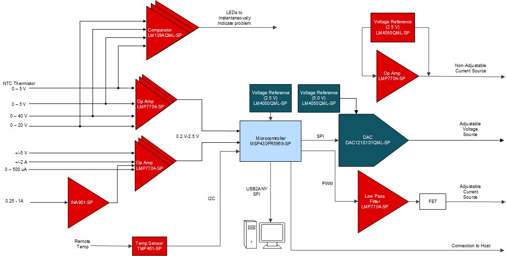
There are 4 main voltage rails that are monitored: 5 V, 20 V, 40 V, and ±5 V. Each rail is measured using the same architecture; starting with a voltage divider to scale the voltage down to within the input limitation of the operational amplifier (op amp), followed by a buffer stage allowing for high input impedance on the sensor side and a low impedance on the ADC side to ensure fast settling time.
There are two options to effectively measure the lower limit of the circuits and remain within the input voltage limitations of the op amp which is approximately 200 mV greater than the negative voltage supply rail.
For the external ADC variation and internal ADC variation, the voltage reference for the offset voltage is the same as the voltage reference for their respective ADC (external, 5 V or internal, 2.5 V). This negates any noise and inaccuracies created by the offset voltage. The second option includes an external negative bias on the negative voltage supply pin of the op amp to decrease the lower input limitation of the op amp.
To help with calculations of the circuit, the Analog Engineer's Calculator was used to calculate resistor and capacitor values. Table 2-3 and Table 2-4 show the calculated values of Ra, Rb, and Rc determined from the gain and voltage output range of the circuit. The calculated resistor values results with a 0-V input having a 0.2-V output, and the maximum voltage input resulting in a 4.8-V output and 2.5-V output for the external ADC or internal ADC configuration, respectively.
RCB and CCB are charge bucket circuits that help with the settling time of the output signal to drive the ADC128S102QML-SP. Due to the MUXed input of the ADC128S102QML-SP the acquisition and conversion time has to be properly calculated. In this design, the desired bandwidth is 5 kHz per channel. This results in 40 kHz of accumulated bandwidth. Finally, to fulfill the Nyquist Theorem, the resulting sampling rate is double the needed bandwidth, resulting in a final sample rate of 80 kHz or 12.5 µs per sample which leads to a minimum conversion time of 10.156 µs and an acquisition time of 2.3437 µs. To help with calculations of the circuit, the Analog Engineer's Calculator was used to calculate RCB and CCB.
 Figure 2-3 Voltage Monitoring - Internal
ADC Configuration
Figure 2-3 Voltage Monitoring - Internal
ADC Configuration| VOLTAGE INPUT (V) | Ra (kΩ) | Rb (kΩ) | Rc (kΩ) | GAIN |
|---|---|---|---|---|
| ±5 | 10 | 115 | 9.09 | 0.46 |
| 5 | 10 | 232 | 232 | 0.92 |
| 20 | 100 | 31.6 | 576 | 0.23 |
| 40 | 100 | 13.7 | 287 | 0.115 |
| VOLTAGE INPUT (V) | Ra (kΩ) | Rb (kΩ) | Rc (kΩ) | GAIN |
|---|---|---|---|---|
| ±5 | 10 | 9.76 | 4.22 | 0.23 |
| 5 | 100 | 97.6 | 576 | 0.46 |
| 20 | 100 | 14.3 | 143 | 0.115 |
| 40 | 100 | 6.65 | 71.5 | 0.0575 |