TIDUEY7 July 2021
- Description
- Resources
- Features
- Applications
- 5
- 1System Description
-
2System Overview
- 2.1 Block Diagram
- 2.2
Design Considerations
- 2.2.1 System Control and Processing
- 2.2.2 Analog Front End
- 2.2.3 Input Voltage Monitoring: 5 V, 20 V, 40 V, and ±5 V
- 2.2.4 Bidirectional Current Sense: ±2 A
- 2.2.5 Unipolar Current Sense: 0.25 A to 1 A
- 2.2.6 TMP461-SP: Local and Remote Temperature Sensing
- 2.2.7 NTC Thermistor Temperature Sensing
- 2.2.8 Adjustable Voltage Source
- 2.2.9 Fixed Output Current Source
- 2.2.10 Adjustable 4-mA Current Source
- 2.2.11 Power Tree and Power Sequencing
- 2.3 Highlighted Products
- 3Hardware, Software, Testing Requirements, and Test Results
- 4Design and Documentation Support
- 5About the Author
2.1 Block Diagram
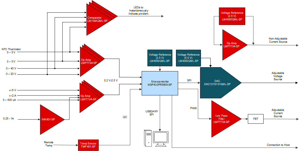
Figure 2-1 and Figure 2-2 illustrate system block diagrams of the external and internal ADC configurations.
 Figure 2-1 System Block Diagram (External
ADC Configuration)
 Figure 2-2 System Block Diagram (Internal
ADC Configuration)