TIDUEY8 March   2023


  1.   Description
  2.   Resources
  3.   Features
  4.   Applications
  5.   5
  6. 1System Description
    1. 1.1 Key System Specifications
  7. 2System Overview
    1. 2.1 Design Block Diagram
    2. 2.2 Highlighted Products
      1. 2.2.1 LMK04832-SP
      2. 2.2.2 LMX2615-SP
      3. 2.2.3 CDCLVP111-SP
      4. 2.2.4 ADC12DJ3200QML-SP
    3. 2.3 Design Steps
      1. 2.3.1 Multiple JESD204B Synchronization Requirements
      2. 2.3.2 Clock Tree Design
        1. 2.3.2.1 Clock Frequency Plan
        2. 2.3.2.2 Clock Tree Components
          1. 2.3.2.2.1 Clock Reference
          2. 2.3.2.2.2 Clock Reference Buffer
          3. 2.3.2.2.3 Clock Distribution
          4. 2.3.2.2.4 Frequency Synthesis
        3. 2.3.2.3 Phase Delay Adjustment Options
        4. 2.3.2.4 Phase-Noise Optimization
        5. 2.3.2.5 Single-Event Effects (SEE) Considerations
        6. 2.3.2.6 Expanding Clock Tree for MIMO Systems
      3. 2.3.3 Power Management
        1. 2.3.3.1 Power Design Considerations
        2. 2.3.3.2 Radiation Hardened (Rad-Hard) Power Tree
          1. 2.3.3.2.1 Radiation-Hardness-Assured (RHA) Load-Switches
          2. 2.3.3.2.2 Radiation-Hardness-Assured (RHA) DC/DC Buck Converter
          3. 2.3.3.2.3 Radiation-Hardness-Assured (RHA) Low-Dropout (LDO) Regulators
            1. 2.3.3.2.3.1 3.3-V Linear Regulator
            2. 2.3.3.2.3.2 4.5-V Linear Regulator
        3. 2.3.3.3 Overcurrent Detection Circuit
  8. 3Getting Started Hardware and Software
    1. 3.1 Hardware Configuration
      1. 3.1.1 Clocking Board Setup
        1. 3.1.1.1 Power Supply
        2. 3.1.1.2 Input Reference Signals
        3. 3.1.1.3 Input sync Signal
        4. 3.1.1.4 Output Signals
        5. 3.1.1.5 Programming Interface
        6. 3.1.1.6 FMC+ Adapter Board Setup
        7. 3.1.1.7 ADC12DJ3200 EVM Setup
        8. 3.1.1.8 TSW14J57EVM Setup
        9. 3.1.1.9 Multichannel Synchronization Setup
    2. 3.2 Software
      1. 3.2.1 Software Required
      2. 3.2.2 Clocking Board Programming Sequence
      3. 3.2.3 ADC12DJ3200CVAL EVM Programming Sequence
      4. 3.2.4 TSW14J57EVM Evaluation Programming Sequence
  9. 4Testing and Results
    1. 4.1 Test Setup
    2. 4.2 Results
      1. 4.2.1 Phase Noise Measurement Results
      2. 4.2.2 Multichannel Clock Phase Alignment
      3. 4.2.3 Signal Chain Performance
      4. 4.2.4 Channel-to-Channel Skew Measurement
    3. 4.3 Summary and Conclusion
  10. 5Design and Documentation Support
    1. 5.1 Design Support
      1. 5.1.1 Schematics
      2. 5.1.2 Bill of Materials
    2. 5.2 Documentation Support
    3. 5.3 Support Resources
    4. 5.4 Trademarks
  11. 6About the Authors
    1. 6.1 Acknowledgments

ADC12DJ3200CVAL EVM Programming Sequence

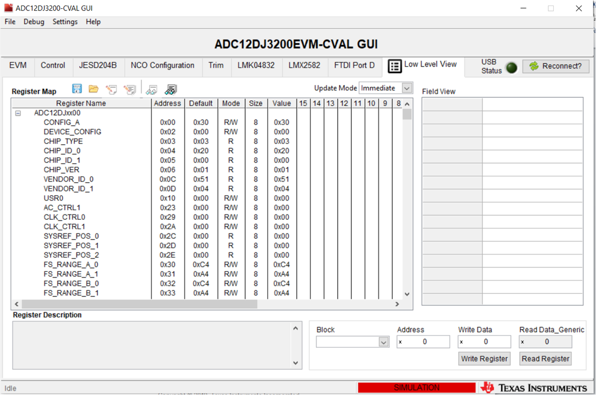
Download the ADC12DJ3200EVM-CVAL GUI from TI.com to program the ADC12DJ3200EVMCVAL. The ADC12DJ3200-SP and LMK04832-SP are devices configured for SNR measurement in the ADC12DJ3200EVMCVAL, as shown in Figure 3-6. The LMK04832 is programmed in distribution mode for the CLKin1 drive to configure SYSREF directly. The ADC12DJ3200EVMCVAL is put into JMODE3 mode to use in dual-channel mode at full Nyquist zone of the device. The EVM is setup in external clock source selection mode, with a sampling frequency of 3200 MSPS and load configuration files in the low level view page of the ADC12DJ3200EVM-CVAL.

Obtain the updated ADC12DJ3200EVM-CVAL configuration files for ADC12DJ3200EVM-CVAL synchronization measurement from the HSDC TIDA01019x GUI software folder.

C:\Program Files (x86)\Texas Instruments\HSDC TIDA01019x GUI\Configuration Files\ ADC12DJ3200EVM-CVAL GUI files

Use the following programming sequence for ADC EVM configuration after the clocking board program:

  1. Load ADCEVM_LMK04832_CLKin1_SYSREF_bypass.cfg
  2. Load ADC12DJxx00_JMODE3_SRC_EN.cfg
  3. Load LMK_LMX_SYSREF_OFF.cfg in HSDC TIDA01019x GUI
  4. Load ADC12DJxx00_JMODE3_SRC_clear.cfg

GUID-20221202-SS0I-CV60-LFCG-CQD51CCVRSVX-low.png Figure 3-6 ADC12DJ3200 EVM Programming