TIDUEY8 March 2023
- Description
- Resources
- Features
- Applications
- 5
- 1System Description
-
2System Overview
- 2.1 Design Block Diagram
- 2.2 Highlighted Products
- 2.3
Design Steps
- 2.3.1 Multiple JESD204B Synchronization Requirements
- 2.3.2 Clock Tree Design
- 2.3.3 Power Management
- 3Getting Started Hardware and Software
- 4Testing and Results
- 5Design and Documentation Support
- 6About the Authors
3.2.2 Clocking Board Programming Sequence
TIDA-010191 clocking board includes the FTDI device, which needs to be programmed once to support the software GUI. An FTDI utility FT-prog is installed from the web. The product description is set to TIDA01019x as shown in Figure 3-4.
 Figure 3-4 Screenshot of the FTDI
Setup
Figure 3-4 Screenshot of the FTDI
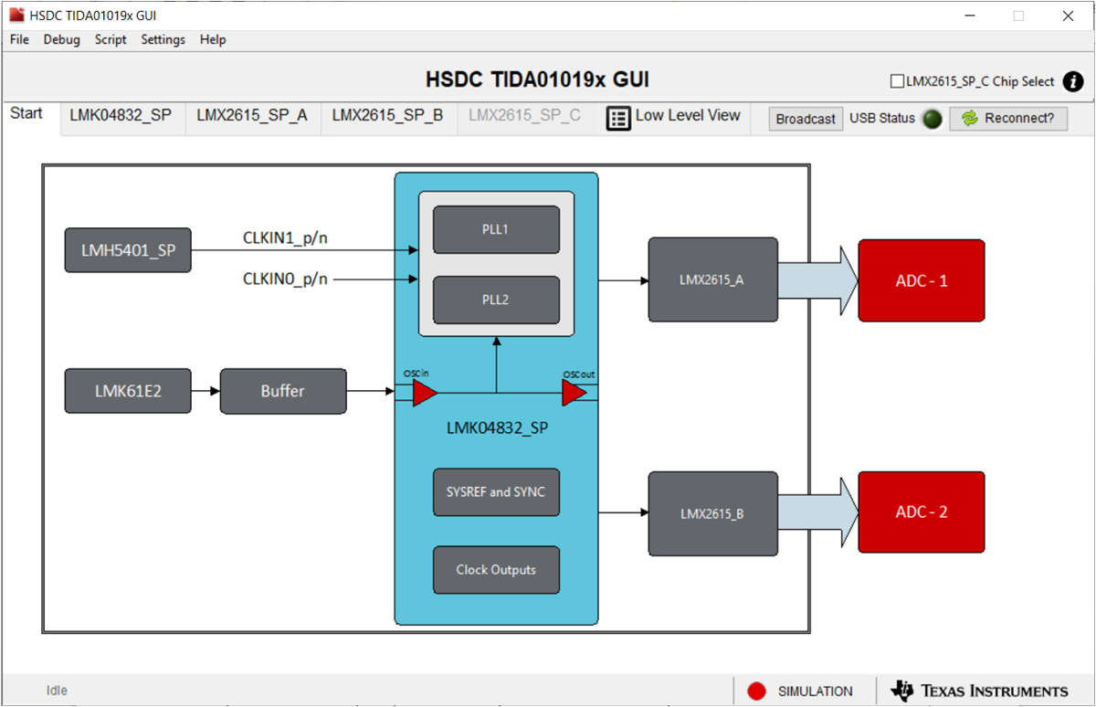
SetupClocking board devices are programmed by HSDC TIDA01019x GUI and can be downloaded from the TIDA-010191 tool page.
 Figure 3-5 Clock GUI
All devices are configured by loading the configuration files in the low level view page.
- To measure LMX2615-SP phase
noise, configure the following:
- External reference at 100 MHz provided through Wenzel source
- The LMX2615-SP devices are taking a reference via CDCLVP111-SP. The LMX2615-SP is programmed for a 100-MHz reference and 200-MHz phase detector frequency at various frequencies to measure the phase noise
- To measure clock skew,
configure the following:
- The LMK61E2 is programmed at 100 MHz. Configure the file in the low level view page
- The LMK04832-SP is programmed in single PLL mode with 100-MHz reference and generates 20-MHz SYSREF frequency and provides the SYSREFREQ and SYNC signals to both LMX2615-SP devices
- Both LMX2615-SP devices are programmed with the common configuration file at a 100-MHz phase detector frequency and generate a 3.2-GHz RFoutA and SYSREF in repeater mode at 20-MHz SYSREFout (RFoutB) from both devices
- To measure the ADC12DJ3200-SP
SNR and skew between multiple ADC EVMs, configure the following:
- The LMK61E2 is
programmed at 100 MHz. Configure the file in the low level view
page
- LMK61E2_100M.cfg
- LMK61E2_EEPROM_Write.cfg
- The LMK04832-SP is
programmed in single PLL mode with 100-MHz reference and generates
20-MHz SYSREF frequency and provides the SYSREFREQ and SYNC signals
to both LMX2615-SP devices. The device also generates the FPGA
clocks and FPGA SYSREFs for TSW14J57 capture cards
- Load LMK04832-SP_160MFCLK_20MSYSREF_100MREF.cfg
- Both LMX2615-SP
devices are programmed with the common configuration file at a
100-MHz phase detector frequency and generate a 3.2-GHz RFoutA and
SYSREF in repeater mode at 20-MHz SYSREFout (RFoutB) from both
devices
- LMX2615-SP_AB_3.2G_100MREF_SYSREF_Repeater.cfg
- The LMK61E2 is
programmed at 100 MHz. Configure the file in the low level view
page