TIDUEY8 March   2023


  1.   Description
  2.   Resources
  3.   Features
  4.   Applications
  5.   5
  6. 1System Description
    1. 1.1 Key System Specifications
  7. 2System Overview
    1. 2.1 Design Block Diagram
    2. 2.2 Highlighted Products
      1. 2.2.1 LMK04832-SP
      2. 2.2.2 LMX2615-SP
      3. 2.2.3 CDCLVP111-SP
      4. 2.2.4 ADC12DJ3200QML-SP
    3. 2.3 Design Steps
      1. 2.3.1 Multiple JESD204B Synchronization Requirements
      2. 2.3.2 Clock Tree Design
        1. 2.3.2.1 Clock Frequency Plan
        2. 2.3.2.2 Clock Tree Components
          1. 2.3.2.2.1 Clock Reference
          2. 2.3.2.2.2 Clock Reference Buffer
          3. 2.3.2.2.3 Clock Distribution
          4. 2.3.2.2.4 Frequency Synthesis
        3. 2.3.2.3 Phase Delay Adjustment Options
        4. 2.3.2.4 Phase-Noise Optimization
        5. 2.3.2.5 Single-Event Effects (SEE) Considerations
        6. 2.3.2.6 Expanding Clock Tree for MIMO Systems
      3. 2.3.3 Power Management
        1. 2.3.3.1 Power Design Considerations
        2. 2.3.3.2 Radiation Hardened (Rad-Hard) Power Tree
          1. 2.3.3.2.1 Radiation-Hardness-Assured (RHA) Load-Switches
          2. 2.3.3.2.2 Radiation-Hardness-Assured (RHA) DC/DC Buck Converter
          3. 2.3.3.2.3 Radiation-Hardness-Assured (RHA) Low-Dropout (LDO) Regulators
            1. 2.3.3.2.3.1 3.3-V Linear Regulator
            2. 2.3.3.2.3.2 4.5-V Linear Regulator
        3. 2.3.3.3 Overcurrent Detection Circuit
  8. 3Getting Started Hardware and Software
    1. 3.1 Hardware Configuration
      1. 3.1.1 Clocking Board Setup
        1. 3.1.1.1 Power Supply
        2. 3.1.1.2 Input Reference Signals
        3. 3.1.1.3 Input sync Signal
        4. 3.1.1.4 Output Signals
        5. 3.1.1.5 Programming Interface
        6. 3.1.1.6 FMC+ Adapter Board Setup
        7. 3.1.1.7 ADC12DJ3200 EVM Setup
        8. 3.1.1.8 TSW14J57EVM Setup
        9. 3.1.1.9 Multichannel Synchronization Setup
    2. 3.2 Software
      1. 3.2.1 Software Required
      2. 3.2.2 Clocking Board Programming Sequence
      3. 3.2.3 ADC12DJ3200CVAL EVM Programming Sequence
      4. 3.2.4 TSW14J57EVM Evaluation Programming Sequence
  9. 4Testing and Results
    1. 4.1 Test Setup
    2. 4.2 Results
      1. 4.2.1 Phase Noise Measurement Results
      2. 4.2.2 Multichannel Clock Phase Alignment
      3. 4.2.3 Signal Chain Performance
      4. 4.2.4 Channel-to-Channel Skew Measurement
    3. 4.3 Summary and Conclusion
  10. 5Design and Documentation Support
    1. 5.1 Design Support
      1. 5.1.1 Schematics
      2. 5.1.2 Bill of Materials
    2. 5.2 Documentation Support
    3. 5.3 Support Resources
    4. 5.4 Trademarks
  11. 6About the Authors
    1. 6.1 Acknowledgments

TSW14J57EVM Evaluation Programming Sequence

The HSDC Pro software interfaces with the TSW14J57EVM to capture and analyze the digital data from the ADC12DJ3200-SP in SNR measurement and skew measurement.

To operate the TSW14J57EVM tools in primary and secondary mode for skew measurement, follow the README note available in the HSDC TIDA01019x GUI software folder. Next, include the updated firmware, .ini files, and other settings in HSDC Pro GUI folder.

Follow the TSW14J57 JESD204B High-Speed Data Capture and Pattern Generator Card user’s guide for HSDC Pro setup and to capture and analyze the data. The following steps show how to configure the HSDC Pro GUI for capturing the data and operating in primary and secondary mode.

  1. Select ADC12DJxx00_JMODE3_F&K_1_32_sysref.ini to interface with the ADC12DJ3200EVM-CVAL GUI for JMODE3
  2. Set the ADC sampling frequency to 3.2 GHz
  3. Set the ADC input target frequency
  4. For SNR measurement, click on the Capture tab and the data is captured on the screen
  5. For skew measurement, configure one HSDC Pro in primary mode (Test Options) and another in secondary mode.
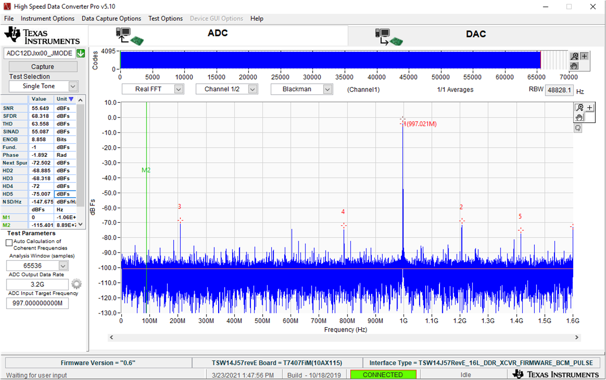
GUID-20221202-SS0I-LWSK-HMHL-CQN1G2186MZN-low.png Figure 3-7 First Test of the Setup by Capturing a Spectrum