TIDUEY8 March   2023


  1.   Description
  2.   Resources
  3.   Features
  4.   Applications
  5.   5
  6. 1System Description
    1. 1.1 Key System Specifications
  7. 2System Overview
    1. 2.1 Design Block Diagram
    2. 2.2 Highlighted Products
      1. 2.2.1 LMK04832-SP
      2. 2.2.2 LMX2615-SP
      3. 2.2.3 CDCLVP111-SP
      4. 2.2.4 ADC12DJ3200QML-SP
    3. 2.3 Design Steps
      1. 2.3.1 Multiple JESD204B Synchronization Requirements
      2. 2.3.2 Clock Tree Design
        1. 2.3.2.1 Clock Frequency Plan
        2. 2.3.2.2 Clock Tree Components
          1. 2.3.2.2.1 Clock Reference
          2. 2.3.2.2.2 Clock Reference Buffer
          3. 2.3.2.2.3 Clock Distribution
          4. 2.3.2.2.4 Frequency Synthesis
        3. 2.3.2.3 Phase Delay Adjustment Options
        4. 2.3.2.4 Phase-Noise Optimization
        5. 2.3.2.5 Single-Event Effects (SEE) Considerations
        6. 2.3.2.6 Expanding Clock Tree for MIMO Systems
      3. 2.3.3 Power Management
        1. 2.3.3.1 Power Design Considerations
        2. 2.3.3.2 Radiation Hardened (Rad-Hard) Power Tree
          1. 2.3.3.2.1 Radiation-Hardness-Assured (RHA) Load-Switches
          2. 2.3.3.2.2 Radiation-Hardness-Assured (RHA) DC/DC Buck Converter
          3. 2.3.3.2.3 Radiation-Hardness-Assured (RHA) Low-Dropout (LDO) Regulators
            1. 2.3.3.2.3.1 3.3-V Linear Regulator
            2. 2.3.3.2.3.2 4.5-V Linear Regulator
        3. 2.3.3.3 Overcurrent Detection Circuit
  8. 3Getting Started Hardware and Software
    1. 3.1 Hardware Configuration
      1. 3.1.1 Clocking Board Setup
        1. 3.1.1.1 Power Supply
        2. 3.1.1.2 Input Reference Signals
        3. 3.1.1.3 Input sync Signal
        4. 3.1.1.4 Output Signals
        5. 3.1.1.5 Programming Interface
        6. 3.1.1.6 FMC+ Adapter Board Setup
        7. 3.1.1.7 ADC12DJ3200 EVM Setup
        8. 3.1.1.8 TSW14J57EVM Setup
        9. 3.1.1.9 Multichannel Synchronization Setup
    2. 3.2 Software
      1. 3.2.1 Software Required
      2. 3.2.2 Clocking Board Programming Sequence
      3. 3.2.3 ADC12DJ3200CVAL EVM Programming Sequence
      4. 3.2.4 TSW14J57EVM Evaluation Programming Sequence
  9. 4Testing and Results
    1. 4.1 Test Setup
    2. 4.2 Results
      1. 4.2.1 Phase Noise Measurement Results
      2. 4.2.2 Multichannel Clock Phase Alignment
      3. 4.2.3 Signal Chain Performance
      4. 4.2.4 Channel-to-Channel Skew Measurement
    3. 4.3 Summary and Conclusion
  10. 5Design and Documentation Support
    1. 5.1 Design Support
      1. 5.1.1 Schematics
      2. 5.1.2 Bill of Materials
    2. 5.2 Documentation Support
    3. 5.3 Support Resources
    4. 5.4 Trademarks
  11. 6About the Authors
    1. 6.1 Acknowledgments

Phase-Noise Optimization

Analog signal chain performance depends on the phase noise and jitter performance of the clock, which can affect the SNR, ENOB, and SFDR, of the data converter. Therefore, optimize the phase noise of the clock to having the lowest jitter.

The LMX2615-SP optimized-loop filter can be programmed to minimize phase noise with the PLLatinum™ simulation tool. In this design, the loop filter are kept the same as LMX2615-SP EVM components.

Table 2-2 LMX2615-SP Design Parameters
PARAMETERVALUE
VCO Gain132 MHz/V

Loop Bandwidth

285 kHz

Phase Margin

65 deg

C1_LF

390 nF

C2_LF

68 nF

C3_LF

Open

C4_LF

1.8 nF

R2

68 Ω

R3_LF

0 Ω

R4_LF

18 Ω

Charge Pump Gain

15 mA

Phase Detector Frequency

200 MHz

VCO Frequency

Designed for 15 GHz, but works over the whole frequency range

The ADC SNR degrades due to external clock jitter and internal ADC aperture jitter. SNR of the ADC, limited by the total jitter, is calculated as:

Equation 1. SNRADC=-20×log2×π×finput×tjitterdBc

To calculate the SNR performance of the ADC12DJ3200-SP over the clocking performance, TI provides a tool with the Jitter and SNR Calculator for ADCs (JITTER-SNR-CALC). Figure 2-7 is a screen-shot with the calculation results:
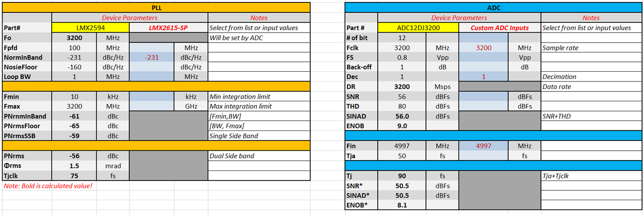
GUID-20221202-SS0I-RD1X-TJCW-SQCCPVHX4GVM-low.pngFigure 2-7 Screen-Shot Jitter to SNR Tool

Figure 2-8 and Figure 2-9 show the relevant SNR plots.


GUID-20221202-SS0I-DJNX-MNHH-BBZPTPKBM6TN-low.svg

Figure 2-8 SNR vs TJ

GUID-20221202-SS0I-9HSZ-SKP0-KZFLN9HN54J1-low.svg

Figure 2-9 SNR vs FIN