TIDUEY8 March   2023


  1.   Description
  2.   Resources
  3.   Features
  4.   Applications
  5.   5
  6. 1System Description
    1. 1.1 Key System Specifications
  7. 2System Overview
    1. 2.1 Design Block Diagram
    2. 2.2 Highlighted Products
      1. 2.2.1 LMK04832-SP
      2. 2.2.2 LMX2615-SP
      3. 2.2.3 CDCLVP111-SP
      4. 2.2.4 ADC12DJ3200QML-SP
    3. 2.3 Design Steps
      1. 2.3.1 Multiple JESD204B Synchronization Requirements
      2. 2.3.2 Clock Tree Design
        1. 2.3.2.1 Clock Frequency Plan
        2. 2.3.2.2 Clock Tree Components
          1. 2.3.2.2.1 Clock Reference
          2. 2.3.2.2.2 Clock Reference Buffer
          3. 2.3.2.2.3 Clock Distribution
          4. 2.3.2.2.4 Frequency Synthesis
        3. 2.3.2.3 Phase Delay Adjustment Options
        4. 2.3.2.4 Phase-Noise Optimization
        5. 2.3.2.5 Single-Event Effects (SEE) Considerations
        6. 2.3.2.6 Expanding Clock Tree for MIMO Systems
      3. 2.3.3 Power Management
        1. 2.3.3.1 Power Design Considerations
        2. 2.3.3.2 Radiation Hardened (Rad-Hard) Power Tree
          1. 2.3.3.2.1 Radiation-Hardness-Assured (RHA) Load-Switches
          2. 2.3.3.2.2 Radiation-Hardness-Assured (RHA) DC/DC Buck Converter
          3. 2.3.3.2.3 Radiation-Hardness-Assured (RHA) Low-Dropout (LDO) Regulators
            1. 2.3.3.2.3.1 3.3-V Linear Regulator
            2. 2.3.3.2.3.2 4.5-V Linear Regulator
        3. 2.3.3.3 Overcurrent Detection Circuit
  8. 3Getting Started Hardware and Software
    1. 3.1 Hardware Configuration
      1. 3.1.1 Clocking Board Setup
        1. 3.1.1.1 Power Supply
        2. 3.1.1.2 Input Reference Signals
        3. 3.1.1.3 Input sync Signal
        4. 3.1.1.4 Output Signals
        5. 3.1.1.5 Programming Interface
        6. 3.1.1.6 FMC+ Adapter Board Setup
        7. 3.1.1.7 ADC12DJ3200 EVM Setup
        8. 3.1.1.8 TSW14J57EVM Setup
        9. 3.1.1.9 Multichannel Synchronization Setup
    2. 3.2 Software
      1. 3.2.1 Software Required
      2. 3.2.2 Clocking Board Programming Sequence
      3. 3.2.3 ADC12DJ3200CVAL EVM Programming Sequence
      4. 3.2.4 TSW14J57EVM Evaluation Programming Sequence
  9. 4Testing and Results
    1. 4.1 Test Setup
    2. 4.2 Results
      1. 4.2.1 Phase Noise Measurement Results
      2. 4.2.2 Multichannel Clock Phase Alignment
      3. 4.2.3 Signal Chain Performance
      4. 4.2.4 Channel-to-Channel Skew Measurement
    3. 4.3 Summary and Conclusion
  10. 5Design and Documentation Support
    1. 5.1 Design Support
      1. 5.1.1 Schematics
      2. 5.1.2 Bill of Materials
    2. 5.2 Documentation Support
    3. 5.3 Support Resources
    4. 5.4 Trademarks
  11. 6About the Authors
    1. 6.1 Acknowledgments

Phase Noise Measurement Results

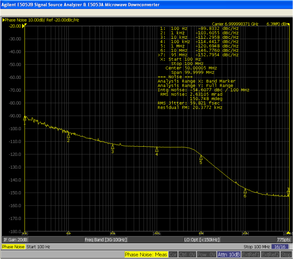
TIDA-010191 clocking board LMX2615-SP devices show almost the same results since both are identical on the board. Table 4-1 shows the measured phase noise performance of the LMX2615-SP at various clock frequencies in the clock board. Measured phase noise plots are shown in Figure 4-5 through Figure 4-7.

Table 4-1 Measured Phase Noise
OUTPUT FREQUENCY (GHz) CONDITION LMX2615-SP DATA SHEET PHASE NOISE (dBc/Hz) TIDA-010191 MEASURED PHASE NOISE (dBc/Hz)
3.5 10-kHz offset –111.5 –112.2
100-kHz offset –115.3 –114.4
1-MHz offset –121.9 –120.6
10-MHz offset –146.3 –146.7
40-MHz offset –150.9 –151.5
9.0 10-kHz offset –104.9 –110
100-kHz offset –111.4 –111.8
1-MHz offset –121.9 –122.3
10-MHz offset –146 –147
40-MHz offset –153 –154
15.0 10-kHz offset –100.8 –106.1
100-kHz offset –107.2 –107.7
1-MHz offset –114.3 –114
10-MHz offset –140.4 –140.8
40-MHz offset –151 –149
GUID-20221202-SS0I-LVB5-B1C6-5DXBWT9LK25V-low.pngFigure 4-5 Phase Noise at 7-GHz Carrier Frequency
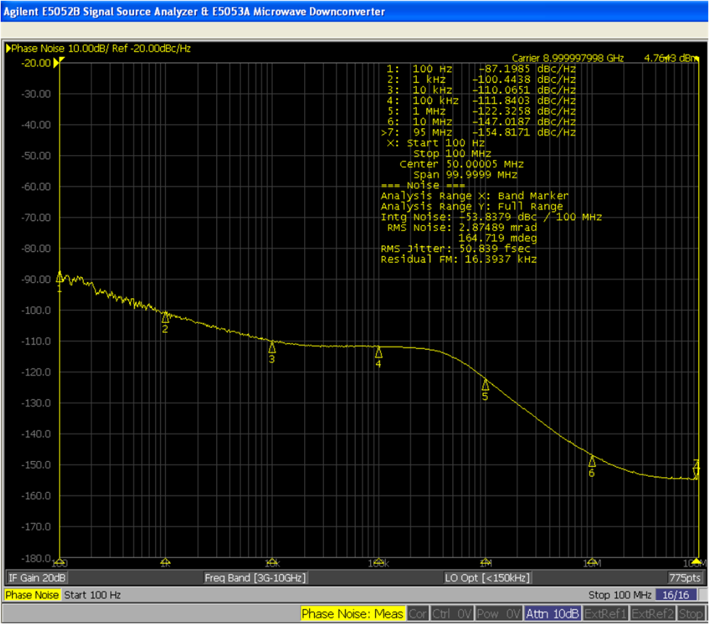
GUID-20221202-SS0I-ZJHZ-SL9S-TXNZTQ2VCPZS-low.pngFigure 4-6 Phase Noise at 9-GHz Carrier Frequency
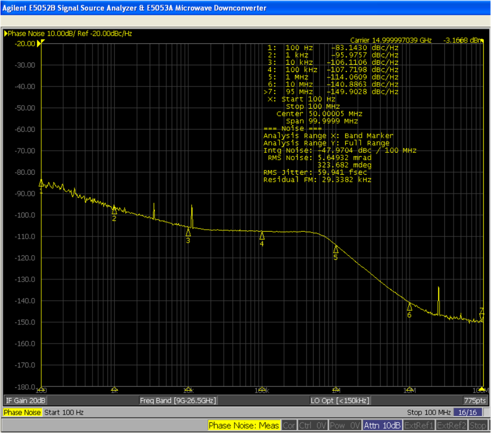
GUID-20221202-SS0I-SW1N-BVTS-TC9J8XB7RQ9K-low.pngFigure 4-7 Phase Noise at 15-GHz Carrier Frequency