TIDUEY8 March   2023


  1.   Description
  2.   Resources
  3.   Features
  4.   Applications
  5.   5
  6. 1System Description
    1. 1.1 Key System Specifications
  7. 2System Overview
    1. 2.1 Design Block Diagram
    2. 2.2 Highlighted Products
      1. 2.2.1 LMK04832-SP
      2. 2.2.2 LMX2615-SP
      3. 2.2.3 CDCLVP111-SP
      4. 2.2.4 ADC12DJ3200QML-SP
    3. 2.3 Design Steps
      1. 2.3.1 Multiple JESD204B Synchronization Requirements
      2. 2.3.2 Clock Tree Design
        1. 2.3.2.1 Clock Frequency Plan
        2. 2.3.2.2 Clock Tree Components
          1. 2.3.2.2.1 Clock Reference
          2. 2.3.2.2.2 Clock Reference Buffer
          3. 2.3.2.2.3 Clock Distribution
          4. 2.3.2.2.4 Frequency Synthesis
        3. 2.3.2.3 Phase Delay Adjustment Options
        4. 2.3.2.4 Phase-Noise Optimization
        5. 2.3.2.5 Single-Event Effects (SEE) Considerations
        6. 2.3.2.6 Expanding Clock Tree for MIMO Systems
      3. 2.3.3 Power Management
        1. 2.3.3.1 Power Design Considerations
        2. 2.3.3.2 Radiation Hardened (Rad-Hard) Power Tree
          1. 2.3.3.2.1 Radiation-Hardness-Assured (RHA) Load-Switches
          2. 2.3.3.2.2 Radiation-Hardness-Assured (RHA) DC/DC Buck Converter
          3. 2.3.3.2.3 Radiation-Hardness-Assured (RHA) Low-Dropout (LDO) Regulators
            1. 2.3.3.2.3.1 3.3-V Linear Regulator
            2. 2.3.3.2.3.2 4.5-V Linear Regulator
        3. 2.3.3.3 Overcurrent Detection Circuit
  8. 3Getting Started Hardware and Software
    1. 3.1 Hardware Configuration
      1. 3.1.1 Clocking Board Setup
        1. 3.1.1.1 Power Supply
        2. 3.1.1.2 Input Reference Signals
        3. 3.1.1.3 Input sync Signal
        4. 3.1.1.4 Output Signals
        5. 3.1.1.5 Programming Interface
        6. 3.1.1.6 FMC+ Adapter Board Setup
        7. 3.1.1.7 ADC12DJ3200 EVM Setup
        8. 3.1.1.8 TSW14J57EVM Setup
        9. 3.1.1.9 Multichannel Synchronization Setup
    2. 3.2 Software
      1. 3.2.1 Software Required
      2. 3.2.2 Clocking Board Programming Sequence
      3. 3.2.3 ADC12DJ3200CVAL EVM Programming Sequence
      4. 3.2.4 TSW14J57EVM Evaluation Programming Sequence
  9. 4Testing and Results
    1. 4.1 Test Setup
    2. 4.2 Results
      1. 4.2.1 Phase Noise Measurement Results
      2. 4.2.2 Multichannel Clock Phase Alignment
      3. 4.2.3 Signal Chain Performance
      4. 4.2.4 Channel-to-Channel Skew Measurement
    3. 4.3 Summary and Conclusion
  10. 5Design and Documentation Support
    1. 5.1 Design Support
      1. 5.1.1 Schematics
      2. 5.1.2 Bill of Materials
    2. 5.2 Documentation Support
    3. 5.3 Support Resources
    4. 5.4 Trademarks
  11. 6About the Authors
    1. 6.1 Acknowledgments

Multichannel Clock Phase Alignment

As explained in Section 3.2.3, synchronized clocks are critical for multichannel systems. This section shows the measured phase aligned clocks and SYSREFs that are generated from both LMX2615-SP devices at a 3.2-GHz device clock and 20-MHz SYSREF. The minimum skew have between the clocks, reflects the minimum channel-to-channel skew in multichannel systems. In this test, the TIDA-010191 clock board shows the clock skew less than 5 ps. As a result, can reduce the channel-to-channel skew in multichannel systems. Figure 4-8 shows the multichannel clock skew measured results from two LMX2615-SP devices at the device clocks and SYSREF signals.
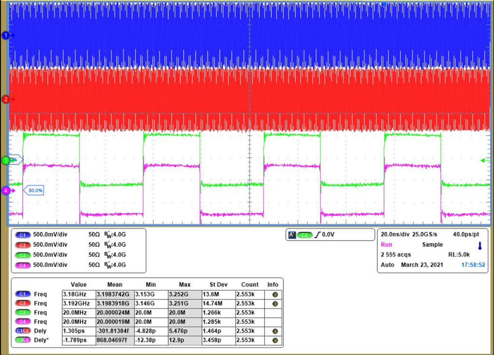
GUID-20221202-SS0I-8NHF-FW9B-9WZDCRJF2JVP-low.png Figure 4-8 Scope-Shot Multichannel Clock Phase Alignment