TIDUEZ1 March 2021
- Description
- Resources
- Features
- Applications
- 5
- 1System Description
-
2System Overview
- 2.1 Block Diagram
- 2.2
Design Considerations
- 2.2.1 Multichannel SSR with Independent Isolation Between SSR Channels
- 2.2.2 Design Challenge With Single Isolation
- 2.2.3 Multichannel SSR Drive With Single Isolation Multichannel Digital Isolator
- 2.2.4 Need of High-Impedance Voltage Translator
- 2.2.5 Design to Minimize Cross-Coupling and MOSFET Gate Pick up Due to Other SSR Switching
- 2.2.6 Schematic: Design of Gate-Drive Circuit
- 2.2.7 Schematic: Digital Isolator Circuit
- 2.2.8 Schematic: 3.3 V to 10V_ISO, 5V_ISO Power Supply
- 2.3 Highlighted Products
- 3Hardware, Software, Testing Requirements, and Test Results
- 4Design and Documentation Support
- 5About the Author
3.3.1 Functional Tests
Figure 3-3 shows the PWM signal from the TIMER and the gate-to-source voltage (VGS) of the SSR MOSFETs. The PWM frequency is 250 kHz and the duty cycle is 34%. The testing is done with the flyback inductor 744889030330 (Wurth). An alternate part is the LPR4012-223DMR (Coil Craft) and in that case the PWM frequency used was around 400 kHz at 34% duty cycle.
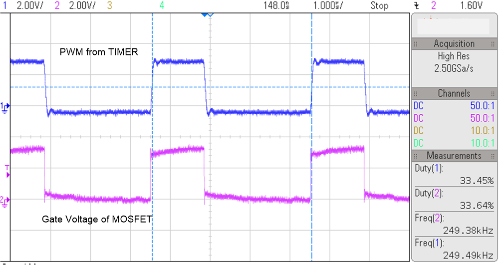 Figure 3-3 PWM Signal from the MCU or
TIMER and MOSFET Gate-Source Voltage
Figure 3-3 PWM Signal from the MCU or
TIMER and MOSFET Gate-Source VoltageFigure 3-4 shows the primary current of the transformer and the voltage across the flyback MOSFET when all the SSRs are ON. The steady-state peak current at the transformer primary is around 135 mA. The peak voltage across the flyback MOSFET is less than 10 V.
 Figure 3-4 Flyback Circuit Voltage and
Current Waveforms - All SSR On
Figure 3-4 Flyback Circuit Voltage and
Current Waveforms - All SSR OnFigure 3-5 shows the primary current of the transformer and the voltage across the flyback MOSFET when all the SSRs are OFF. The steady-state peak current at the transformer primary is around 135 mA. The peak voltage across the flyback MOSFET is less than 10 V.
 Figure 3-5 Flyback Circuit Voltage and
Current Waveforms - All SSR Off
Figure 3-5 Flyback Circuit Voltage and
Current Waveforms - All SSR OffTable 3-1 illustrates the output voltage of the flyback power supply when all the SSR channels are on and all channels are off.
| Operating Condition | Input Voltage | Output Voltage | Input Current on 3.3-V Rail |
|---|---|---|---|
| All SSR channels On | 3.3 V | 7 V | 47 mA |
| All SSR channels Off | 3.3 V | 9.5 V | 56 mA |
Figure 3-6 to Figure 3-9 show the SSR switching with a DC power supply of +40 V and –40 V. During the SSR turn off, the voltage across the SSR MOSFET pair shows spikes due to the inductive kickback from the relay coil and the voltage got clamped to approximately ±46 V, by the bidirectional TVS chip, SMAJ40CA.
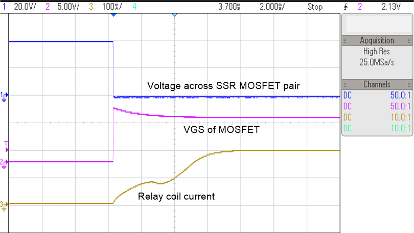 Figure 3-6 SSR Turn on Waveform at 40
V
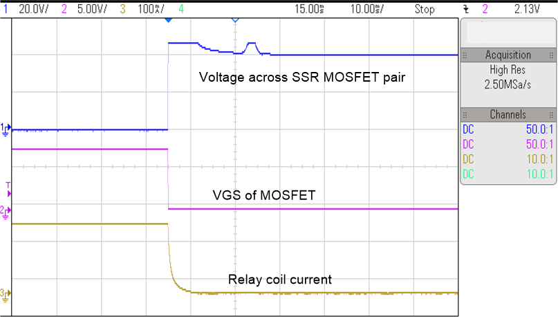 Figure 3-7 SSR Turn off Waveform at
40 V
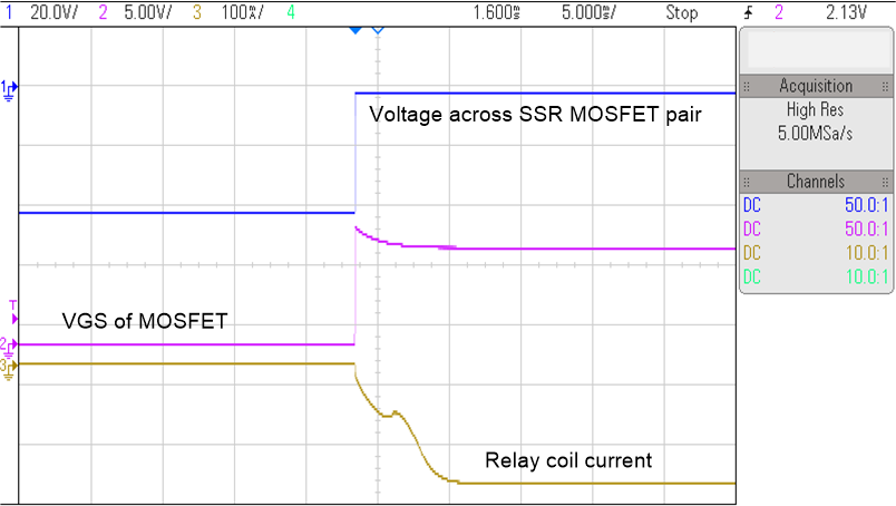 Figure 3-8 SSR Turn on Waveform at
–40 V
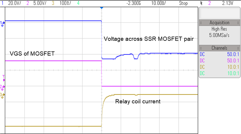 Figure 3-9 SSR Turn off Waveform at
–40 V
Figure 3-9 SSR Turn off Waveform at
–40 VFigure 3-10 and Figure 3-11 show the VGS and VDS slew rate waveforms during MOSFET turn on and turn off. The VDS slew depends on the gate-circuit parameters, the gate resistance, gate-drive voltage, gate-drive PNP transistor saturation current, and so forth. The VDS slew also depends on the load current and load inductance. The FET switching turn on and turn off times are adjustable in hardware and need to be tuned in the application. The VDS slew time is approximately 1–2 µs during turn on and turn off. The turn on slew time can be decreased by increasing the base current of the gate-drive PNP transistor and by reducing the gate resistor. The turn off time can be decreased by decreasing the resistor connected across the gate and source of SSR MOSFETs.
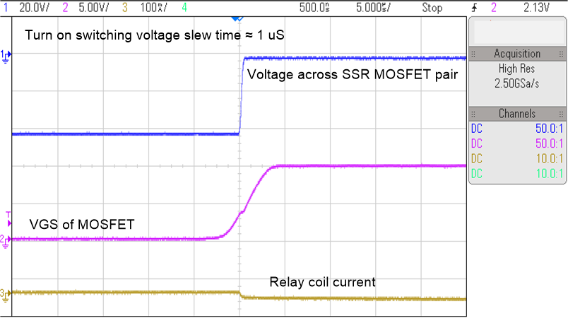 Figure 3-10 MOSFET Turn on Switching
Waveform
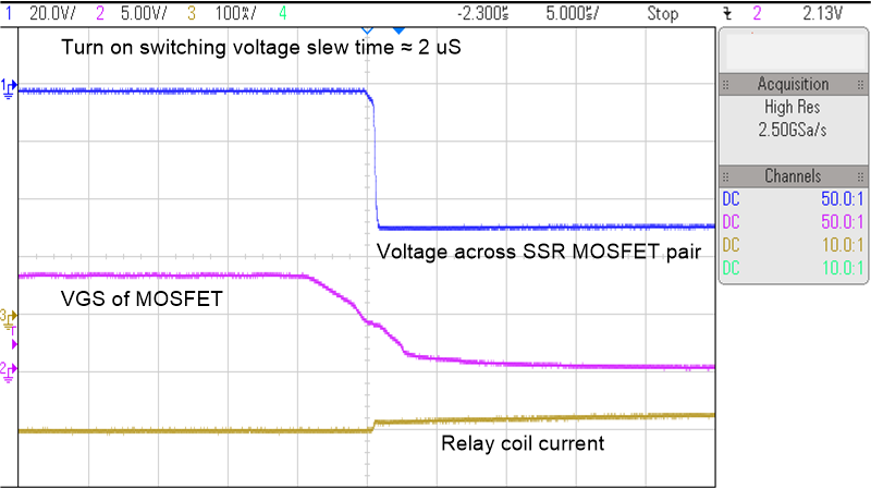 Figure 3-11 MOSFET Turn off Switching
Waveform
 Figure 3-12 and Figure 3-13 show the total turn on and turn off time of the SSR from the control signal toggling to the complete turn on or turn off of the SSR MOSFETs. The turn on and turn off time of the SSR after the turn on and turn off command from control signal (INx signals of digital isolator) is less than 15 µs. The time can be adjusted by changing the MOSFET gate biasing.
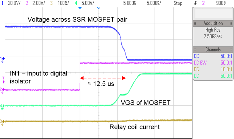 Figure 3-12 Waveforms Showing SSR Turn
on Time
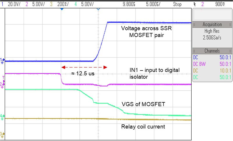 Figure 3-13 Waveforms Showing SSR Turn
off Time
Figure 3-13 Waveforms Showing SSR Turn
off TimeFigure 3-14 and Figure 3-15 show the gate voltage pick up of an SSR channel that is in off state, while another SSR channel is turned on or off. In Figure 3-14, The SSR-2 is in off state. The already on SSR-1 is turned off with negative DC supply voltage, while doing so, the voltage across SSR-1 MOSFET pair changes from 0 V to –40 V in around 2 µs. During this event the gate-to-source pick up voltage (VGS) of SSR-2 MOSFETs is monitored. The VGS pick up of SSR-2 is approximately 100 mV. In Figure 3-15, the SSR-2 is in off state. The already off SSR-1 is turned on with negative DC supply voltage, while doing so, the voltage across SSR-1 MOSFET pair changes from –40 V to 0 V in around 2 µs. During this event the VGS pick up of SSR-2 is approximately 150 mV.
In both the cases, the gate pick-up voltage observed at VGS of the OFF state SSR is less than 200 mV. This ensures that the VGS is well below the threshold voltage of the MOSFET (VGS_th = 2.4 V at 150°C for CSD19538Q2) ensure very good design margin. In other way, the design has least cross-coupling between channels ensuring a reliable independent control of SSR.
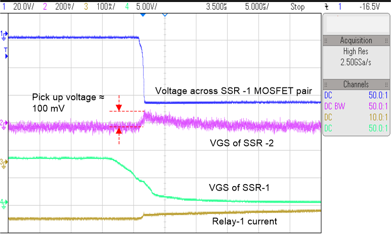 Figure 3-14 Test Waveforms Showing
Least Cross-Coupling During SSR Turn Off
 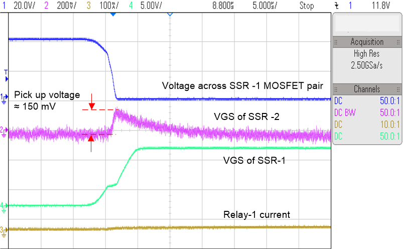 Figure 3-15 Test Waveforms Showing
Least Cross-Coupling During SSR Turn On
Figure 3-15 Test Waveforms Showing
Least Cross-Coupling During SSR Turn OnFigure 3-16 shows the independent control of two SSR channels with a 24-V AC supply. A 120 VAC to 24 VAC, 20VA transformer is used to provide the 24-VAC power supply to the SSR.
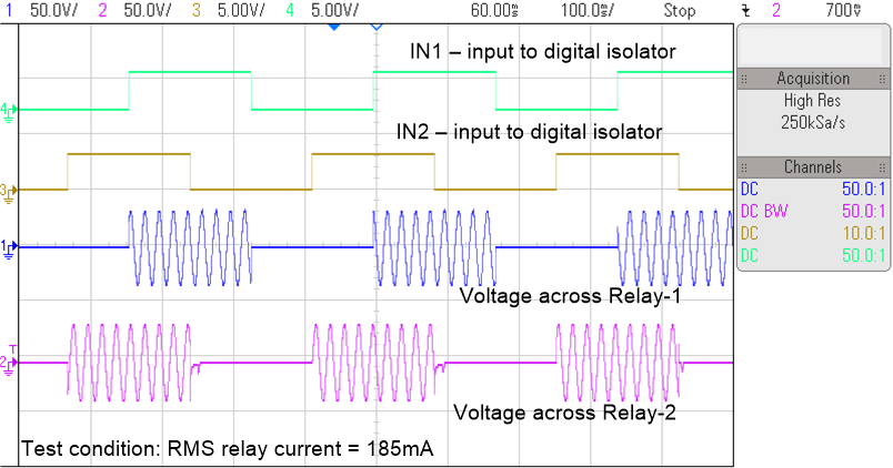 Figure 3-16 Test Waveforms at 24-VAC
Supply - Independent Operation of SSR