TIDUEZ1 March 2021
- Description
- Resources
- Features
- Applications
- 5
- 1System Description
-
2System Overview
- 2.1 Block Diagram
- 2.2
Design Considerations
- 2.2.1 Multichannel SSR with Independent Isolation Between SSR Channels
- 2.2.2 Design Challenge With Single Isolation
- 2.2.3 Multichannel SSR Drive With Single Isolation Multichannel Digital Isolator
- 2.2.4 Need of High-Impedance Voltage Translator
- 2.2.5 Design to Minimize Cross-Coupling and MOSFET Gate Pick up Due to Other SSR Switching
- 2.2.6 Schematic: Design of Gate-Drive Circuit
- 2.2.7 Schematic: Digital Isolator Circuit
- 2.2.8 Schematic: 3.3 V to 10V_ISO, 5V_ISO Power Supply
- 2.3 Highlighted Products
- 3Hardware, Software, Testing Requirements, and Test Results
- 4Design and Documentation Support
- 5About the Author
2.2.4 Need of High-Impedance Voltage Translator
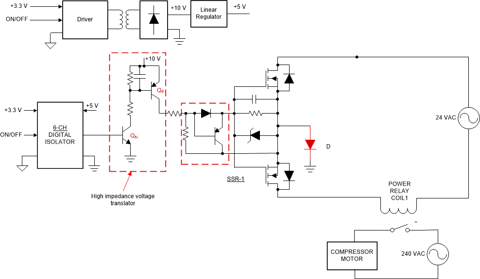
The reference design SSR topology uses the high impedance voltage translator connected between the digital isolator and the SSR MOSFET gate. Figure 2-7 illustrates the high-impedance voltage translator consists of a PNP transistor (QP) and an NPN transistor (QN).
 Figure 2-7 High Impedance Voltage
Translator for Driving Multiple SSR With Single Isolating Element
Figure 2-7 High Impedance Voltage
Translator for Driving Multiple SSR With Single Isolating ElementThe NPN and the PNP transistor circuit forms the voltage translator circuit, translating the 5 V at the digital isolator output to a higher voltage for the MOSFET gate drive. It is also required that the off-state leakage of the PNP transistor has to be very low so that the resulting voltage drop across the resistor between the gate and source of the SSR MOSFET, is sufficiently less than the worst-case gate threshold voltage of MOSFETs.