TIDUEZ6 December 2021 TPS62912 , TPS62913
- Description
- Resources
- Features
- Applications
- 5
- 1System Overview
- 2Hardware, Software, Testing Requirements, and Test Results
- 3Design and Documentation Support
- 4About the Author
- 5Acknowledgement
1.4.1.1 RF Transceiver Synchronization Challenges
In a JESD204B system environment, data transfer from the JESD204B RX block to the TX block happens in multi-frames. These multi-frames are aligned to the edges of the local multi-frame clock (LMFC), which is internal to the JESD204B RX and TX block. The concept of the LMFC and the associated alignment requirements are critical in applications that require deterministic latency and multiple device synchronization. To achieve deterministic latency, multiple device synchronization, or both is to ensure that the LMFC of each JESD204B device in the JESD204B system environment are aligned. The LMFC of each JESD204B device is aligned through the SYSREF signal, which is globally generated from the common source throughout the JESD204B system. Once the LMFCs of all devices in the system are aligned, the devices are synchronized and data transfer happens at the same rate and at the same instant.
High-speed applications like RADAR and electronic warfare, where multiple channels are needed to achieve higher data rates or multiple input and multiple outputs (MIMO), require a multichannel device to reduce system size, complexity, and cost. The AFE7950, a JESD204B-compliant device, supports 4-transmit and 4-receive signal chains and is a good fit for these multichannel systems with the provided clock solution. A large number of AFE7950 devices can be used in such systems requiring multiple device synchronization.
The key clocking challenges in multi-RF transceiver systems to minimize channel-to-channel skew include:
- Synchronization of device clocks for RF transceivers
- Synchronization of digital functions across RF transceivers
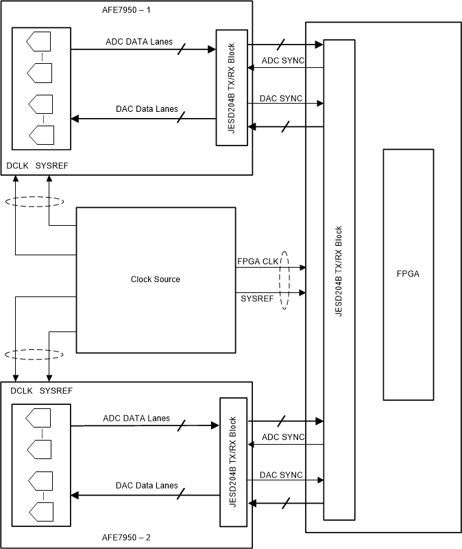
Figure 1-2 shows the typical setup for multiple JESD204B TX and RX device synchronization. For synchronization, the clock source requires:
- Phase-align device clocks and sampling clocks (DCLK) at each AFE7950 device
- In-phase SYSREF to each DCLK to meet SYSREF setup and hold time of the AFE7950
- In-phase FPGA CLK and FPGA SYSREF, if using multiple FPGAs in a system
AFE7950 internal clocks, such as ADC sampling clock, frame clock, or LMFC, are generated from the common DCLK. Hence the DCLK phase is critical to each data converter for multiple synchronized systems.
 Figure 1-2 Synchronization Block
Diagram