TIDUEZ6 December   2021 TPS62912 , TPS62913


  1.   Description
  2.   Resources
  3.   Features
  4.   Applications
  5.   5
  6. 1System Overview
    1. 1.1 Key System Level Specifications
    2. 1.2 System Description
    3. 1.3 Block Diagram
    4. 1.4 Design Considerations
      1. 1.4.1 Frequency Band and Applications
        1. 1.4.1.1 RF Transceiver Synchronization Challenges
        2. 1.4.1.2 JESD204B-Compliant Multichannel Phase Synchronized Clocks Generation
      2. 1.4.2 Clock Jitter and System SNR
      3. 1.4.3 Power-Supply Selection
      4. 1.4.4 Highlighted Products
        1. 1.4.4.1 AFE7950
        2. 1.4.4.2 LMX2820
        3. 1.4.4.3 LMK04832
        4. 1.4.4.4 TPS62913 and TPS62912
        5. 1.4.4.5 LMK1C1104
  7. 2Hardware, Software, Testing Requirements, and Test Results
    1. 2.1 Required Hardware and Software
      1. 2.1.1 Hardware
        1. 2.1.1.1 Clocking Board Setup
        2. 2.1.1.2 FMC-to-FMC Adapter Board Setup
        3. 2.1.1.3 AFE7950EVM Setup
        4. 2.1.1.4 TSW14J56EVM Setup
        5. 2.1.1.5 Hardware Setup of Multiple Transceiver Synchronization
      2. 2.1.2 Software
        1. 2.1.2.1 TIDA-010230 Clocking Board GUI
        2. 2.1.2.2 AFE7950 EVM GUI
        3. 2.1.2.3 High-Speed Data Converter (HSDC) Pro
        4. 2.1.2.4 Programming Steps
        5. 2.1.2.5 Clocking Board Programming Sequence
        6. 2.1.2.6 Latte SW and HSDC Pro Setup
    2. 2.2 Test Setup
    3. 2.3 Test Results
      1. 2.3.1 LMX2820 Phase-Noise Performance
      2. 2.3.2 AFE7950 Transmitter Performance
      3. 2.3.3 AFE7950 Receiver Performance
      4. 2.3.4 Multiple AFE7950s TX and RX Alignment
      5. 2.3.5 Summary and Conclusion
  8. 3Design and Documentation Support
    1. 3.1 Design Files
      1. 3.1.1 Schematics
      2. 3.1.2 BOM
    2. 3.2 Tools and Software
    3. 3.3 Documentation Support
    4. 3.4 Support Resources
    5. 3.5 Trademarks
  9. 4About the Author
  10. 5Acknowledgement

Clock Jitter and System SNR

The ADC SNR degrades due to external clock jitter and internal ADC aperture jitter. SNR of the ADC, limited by the total jitter, is calculated as in Equation 1:

Equation 1. ( S N R ) j i t t e r = - 20 log 2 π f i n T j i t t e r [ i n   d B c ]

SNR of the ADC is also affected by the quantization noise of the ADC, thermal noise, and jitter. The effective SNR of ADC that includes all of these artifacts can be represented using Equation 2:

Equation 2. (SNR)ADC=-20log10-SNRquantization_noise202+10-SNRthermal_noise202+10-SNRjitter202  [in dBc]

Figure 1-5 shows the effective SNR of a 14-bit ADC from Texas Instruments. The external clock jitter depends on the clock generator section and should be designed in such a way that it is not limiting the ADC SNR performance.
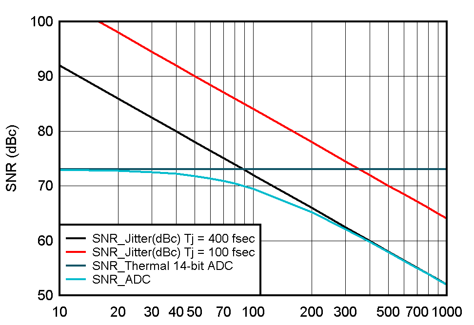
GUID-20211108-SS0I-HM3R-DCKM-QWLC8JG6MPXT-low.gif Figure 1-5 SNR Performance vs Input Frequency