TIDUEZ8C december   2022  – june 2023


  1.   1
  2.   Description
  3.   Resources
  4.   Features
  5.   Applications
  6.   6
  7. 1System Description
    1. 1.1 Insulation Monitoring
    2. 1.2 Impact of Parasitic Isolation Capacitance
    3. 1.3 IEC 61557-8 Standard for Industrial Low-Voltage Distribution Systems
    4. 1.4 Key System Specifications
  8. 2System Overview
    1. 2.1 Block Diagram
    2. 2.2 Highlighted Products
      1. 2.2.1 TPSI2140
      2. 2.2.2 AMC3330
      3. 2.2.3 TPS7A24
      4. 2.2.4 REF2033
      5. 2.2.5 TLV6001
    3. 2.3 Design Considerations
      1. 2.3.1 Resistive Bridge
      2. 2.3.2 Isolated Analog Signal Chain
        1. 2.3.2.1 Differential to Single-Ended Conversion
        2. 2.3.2.2 High-Voltage Measurement
        3. 2.3.2.3 Signal Chain Error Analysis
      3. 2.3.3 Loss of PE Detection
      4. 2.3.4 Insulation Monitoring on AC Lines
      5. 2.3.5 PCB Layout Recommendations
  9. 3Hardware, Software, Testing Requirements, and Test Results
    1. 3.1 Hardware Requirements
      1. 3.1.1 Connectors
      2. 3.1.2 Default Jumper Configuration
      3. 3.1.3 Prerequisites
    2. 3.2 Software Requirements
    3. 3.3 Software
    4. 3.4 Test Setup
    5. 3.5 Test Results
  10. 4Design and Documentation Support
    1. 4.1 Design Files
      1. 4.1.1 Schematics
      2. 4.1.2 BOM
    2. 4.2 Documentation Support
    3. 4.3 Support Resources
    4. 4.4 Trademarks
  11. 5About the Author
  12. 6Revision History

REF2033

The REF20XX are a family of dual-output, VREF and VBIAS (VREF / 2) band-gap voltage references. Figure 2-5 provides a block diagram of the basic band-gap topology and the two buffers used to derive the VREF and VBIAS outputs. Transistors Q1 and Q2 are biased such that the current density of Q1 is greater than that of Q2 . The difference of the two base emitter voltages (VBE1 – VBE2) has a positive temperature coefficient and is forced across resistor R5 . The voltage is amplified and added to the base emitter voltage of Q2 , which has a negative temperature coefficient. The resulting band-gap output voltage is almost independent of temperature. Two independent buffers are used to generate VREF and VBIAS from the band-gap voltage. The resistors R1 , R2 and R3 , R4 are sized such that VBIAS = VREF / 2.

The e-Trim™ integrated circuit, which is a method of package-level trim for the initial accuracy and temperature coefficient of VREF and VBIAS, implemented during the final steps of manufacturing after the plastic molding process. This method minimizes the influence of inherent transistor mismatch, as well as errors induced during package molding. e-Trim is implemented in the REF20xx to minimize the temperature drift and maximize the initial accuracy of both the VREF and VBIAS outputs.
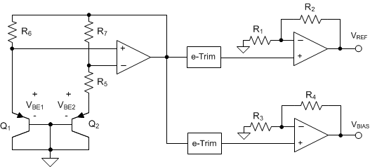
GUID-33BFAB8C-E59B-4587-952B-E5840ED39A82-low.gif Figure 2-5 REF2033 Functional Block Diagram