TIDUF04 December 2022
- Description
- Resources
- Features
- Applications
- 5
- 1System Description
-
2System Overview
- 2.1 Block Diagram
- 2.2
Design Considerations
- 2.2.1
Isolated AC/DC Power Supply Design
- 2.2.1.1 Input Bulk Capacitance and Minimum Bulk Voltage
- 2.2.1.2 Transformer Turns-Ratio, Primary Inductance, and Primary Peak Current
- 2.2.1.3 Transformer Parameter Calculations: Primary and Secondary RMS Currents
- 2.2.1.4 Main Switching Power MOSFET Selection
- 2.2.1.5 Rectifying Diode Selection
- 2.2.1.6 Output Capacitor Selection
- 2.2.1.7 Capacitance on VDD Pin
- 2.2.1.8 Open-loop Voltage Regulation Versus Pin Resistor Divider, Line Compensation Resistor
- 2.2.1.9 Feedback Elements
- 2.2.1.10 Backup Power Supply
- 2.2.1.11 Supercapacitor Selection
- 2.2.1.12 Supercapacitor Charger Design
- 2.2.2 Control Pilot Signal Interface
- 2.2.3 Relay Drive and Weld Detect
- 2.2.4 Residual Current Detection
- 2.2.1
Isolated AC/DC Power Supply Design
- 2.3 Highlighted Products
- 3Hardware, Testing Requirements, and Test Results
- 4Design and Documentation Support
- 5About the Author
2.2.4.5 Filter Stage
The three goals of filter stage are to gain the ground fault detection signal, filter the noise created by the auto-oscillation circuit, and correct a DC bias inherent to the fluxgate core. The filter filters noise in the signal path from the burden resistor to the ADC. Too much noise can trigger false trips. The major source of noise is switching noise caused by the auto-oscillation circuit generating switching of the DRV8220. The auto-oscillation switching frequency changes with fluxgate sensor permeability, burden resistance, or adjusting the saturation detection circuit. The Hitachi nanocrystalline cores used for testing ranged from 600 Hz to 800 Hz with a 1-kΩ burden resistor.
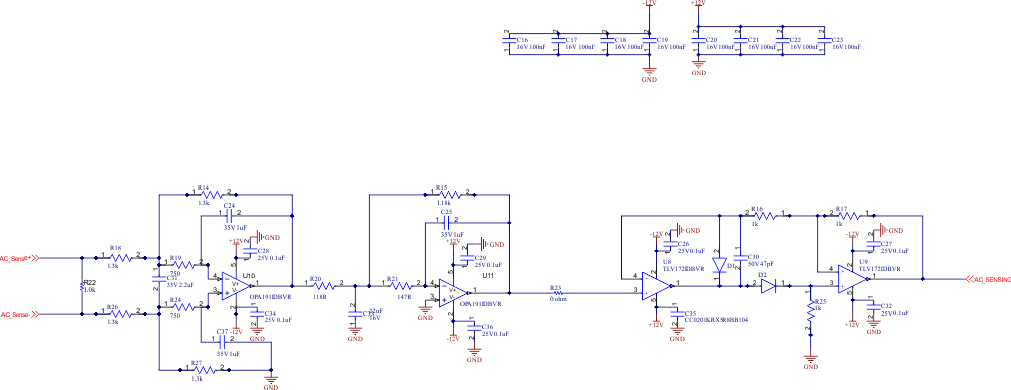
During a fault, the filter stage outputs a detectable signal read by the ADC. A fault trip occurs when the filter stage output signal passes a threshold and the MCU determines the fault type, as AC and DC faults have separate trip thresholds adjustable within software. In this design with a gain of 20 dB, a DC fault of 6-mA outputs a 200-mV offset. An AC fault of 30-mARMS outputs a peak of 600 mV. The gain can be increased, make sure the trip threshold is below the rail of op amps. The filter stage is designed to gain the fault signal by 20 dB and attenuate frequencies above 70 Hz. The filter stage consists of four subsections: differential to single end, low-pass filter, full-wave rectifier, and a DC offset circuit in place of R23.
 Figure 2-11 Filter Stage
Schematic
Figure 2-11 Filter Stage
SchematicThe filter topology used is the Multiple FeedBack (MFB) topology and is often preferred due to low sensitivity to component variations. The MFB topology creates an inverting second-order stage. This inversion can be a concern in the filter application. The MFB filter circuit can be configured as a low-pass filter, high-pass filter, or band-pass filter based on the component selection. For this application, a fourth-order low-pass filter with a Butterworth response was used.