TIDUF08 January 2024
- 1
- Description
- Resources
- Features
- Applications
- 6
- 1System Description
- 2System Overview
- 3Hardware
- 4Design and Documentation Support
2.3.3.3 Thermal Considerations
An important consequence of the efficiency numbers shown in Figure 2-5 is that it enables to perform DLPA2005 thermal calculations. Since the efficiency is not 100%, power is dissipated in the DLPA2005 chip. Due to that dissipation, die temperature rises. For reliability reasons, is good to aim for as low as possible die temperatures. Using a heat sink and airflow are efficient means to keep die temperature reasonably low. In cases that airflow and or a heat sink are or is not feasible, the system designer must specifically pay attention to the thermal design. The die temperature for regular operation needs to remain below 120°C.
") Figure 2-5 Measured
Typical Power Converter Efficiency as a Function of ILED for
Several Supply Voltages (VOUTmax = 4.8 V for Each
Supply)
Figure 2-5 Measured
Typical Power Converter Efficiency as a Function of ILED for
Several Supply Voltages (VOUTmax = 4.8 V for Each
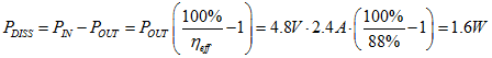
Supply)In the following, an example is given of such a thermal calculation. The calculation starts with summarizing all blocks in the DLPA2005 that dissipate. The buck-boost converter supplying the LED power is the main source of dissipation. For illustrating purposes, we assume this buck-boost converter to be the only block that dissipates significantly. For the example assume: VOUT = 4.8 V (for all three LEDs), IOUT = 2.4 A and VIN = 5 V. From Figure 2-5 it can be derived that the related efficiency equals about neff = 88%.
The power dissipated by the DLPA2005 is then given by:
The rise of die temperature due to this power dissipation can be calculated using the thermal resistance from junction to ambient, JA=27.9°C/W. This calculation yields:

It is also possible to calculate the maximum allowable ambient temperature to prevent surpassing the maximum die temperature. Assume again the dissipation of PDISS=1.6W. The maximum ambient temperature that is allowed is then given by:

It is again stressed that for proper calculations, the total power dissipation of the DLPA2005 needs to be taken into account. Also, if components that are close to the DLPA2005 also dissipate a significant amount of power, the (local) ambient temperature can be higher than the ambient temperature of the system.
If calculations show that the die temperature can surpass the maximum specified value, two basic options exist:
- Adding a heat sink with or without airflow. This reduces 0JA yielding lower die temperature.
- Lowering the dissipation in the DLPA2005 implying lowering the maximum allowable LED current.