TIDUF08 January 2024
- 1
- Description
- Resources
- Features
- Applications
- 6
- 1System Description
- 2System Overview
- 3Hardware
- 4Design and Documentation Support
2.3.2 FPGA DDR2 SDRAM Interface Routing
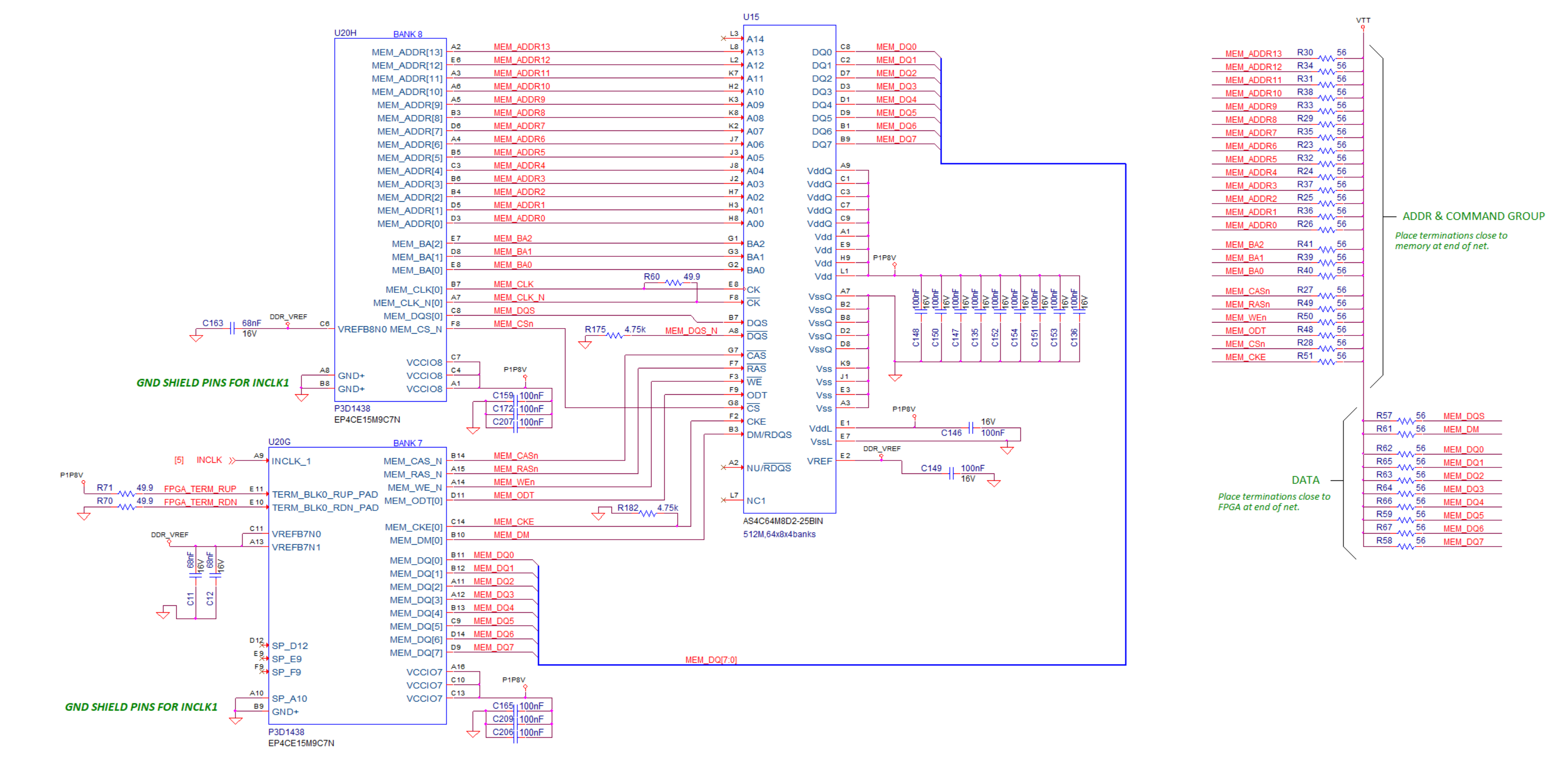
The FPGA to DDR2 SDRAM interface is based on a 400-MHz DDR clock rate. The Intel® Cyclone® IV E FPGA (EP4CE15M9C7N) to an Alliance DDR2 SDRAM (AS4C64M8D2-25BIN) interface diagram is shown in Figure 2-3 and the recommended interface layout guidelines are defined in Table 2-5.
 Figure 2-3 FPGA-DDR2 Interface
Table 2-5 Recommended FPGA-DDR2 PCB Matching and
Trace Delays
| GROUP | GROUP NAME | LENGTH MATCH WITHIN GROUP | LENGTH MATCH TO OTHER SIGNALS | ADDITIONAL ROUTING REQUIREMENTS |
|---|---|---|---|---|
| MEM_ADDR[13:0], MEM_BA[2:0], MEM_CASn, MEM_RASn, MEM_WEn, MEM_ODT MEM_CKE, MEM_CSn | Addr/Cntl Group | WITHIN GROUP ±50 ps | 0 ps to 15 ps less than MEM_CLK and MEM_CLK_N | 50 Ω - place termination at DDR2 end of trace - maximum length 250 ps - minimum length 200 ps |
| MEM_DQ[7:0], MEM_DM, MEM_DQS | Data Group | WITHIN GROUP ±10 ps | MEM_CLK, MEM_CLK_N ±10 ps | 50 Ω - use inner layer - route on same layer - place termination at FPGA end of trace - max length 250 ps - min length 200 ps |
| MEM_CLK, MEM_CLK_N | CLK Group | WITHIN GROUP ±2 ps | MEM_DQS ±2 ps Must be 0 ps to 15 ps longer than ADDR & CNTL Group | 100 differential - minimize trace on outer layer - use inner layer - max length 250 ps - min length 200 ps |
PCB routing best practices:
- Use inner PCB layers when possible
- Route DDR_DQ(7:0), MEM_DM and DDR_DQS on the same layers