TIDUF08 January 2024
- 1
- Description
- Resources
- Features
- Applications
- 6
- 1System Description
- 2System Overview
- 3Hardware
- 4Design and Documentation Support
2.3.1.1 PLL Power Layout
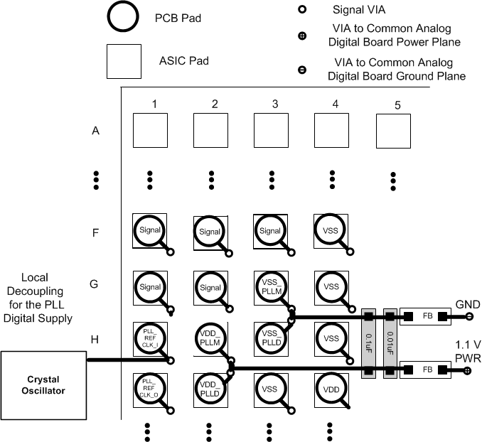
Follow these recommended guidelines to achieve acceptable controller performance for the internal PLL. The DLPC1438 controller contains two internal PLLs which have dedicated analog supplies (VDD_PLLM, VSS_PLLM, VDD_PLLD, and VSS_PLLD). At a minimum, isolate the VDD_PLLx power and VSS_PLLx ground pins using a simple passive filter consisting of two series ferrite beads and two shunt capacitors (to widen the spectrum of noise absorption). TI recommends that one capacitor be 0.1 µF and one be 0.01 µF. Place all four components as close to the controller as possible. Keep the leads of the high-frequency capacitors as short as possible. Connect both capacitors from VDD_PLLM to VSS_PLLM and VDD_PLLD to VSS_PLLD on the controller side of the ferrite beads. Select ferrite beads with these characteristics:
- DC resistance less than 0.40 Ω
- Impedance at 10 MHz equal to or greater than 180 Ω
- Impedance at 100 MHz equal to or greater than 600 Ω
The PCB layout is critical to PLL performance. It is vital that the quiet ground and power are treated like analog signals. Therefore, VDD_PLLM and VDD_PLLD must be a single trace from the DLPC3436 controller to both capacitors and then through the series ferrites to the power source. Make the power and ground traces as short as possible, parallel to each other, and as close as possible to each other.
 Figure 2-2 PLL Filter
Layout