TIDUF12 December 2022
5.1.3.1 20 GHz (FMCW) RF LO Sync
This reference design is based on TI’s AWR2243 radar chip. Using the 20 GHz LO input and output paths, two of these chips are cascaded together and operated synchronously. This requires that the RF LO frequencies of each chip be synchronized. The AWR2243 synthesizer generates LO between 19 GHz and 20.25 GHz, depending on the programmed chirp RF output frequencies.
The AWR2243 that is designated as the primary, generates a common Local Oscillator (LO) signal (19 GHz to 20.25 GHz) to be shared across all the transmitters and receivers in the entire cascade system.
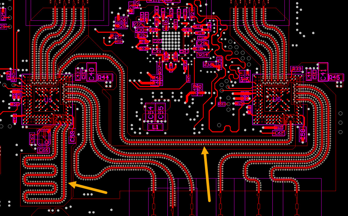
The primary AWR2243 is capable of supplying the shared LO signal on two different output pins through two different delay matched amplifiers. Either or both of these signals, FM_CW_CLKOUT and FM_CW_SYNCOUT, can be used as the source of the LO from the primary to the secondary device. To avoid skew between the LO signals used in both devices, the LO signal input into the primary needs to pass through a trace that is length-matched to the trace between the primary and the secondary devices. As shown in Figure 5-2, one LO signal output is routed with a trace between devices. Then, the other output LO signal from the primary device is looped back to the LO signal input on the primary device using a trace that is the same length.
 Figure 5-1 LO Clock Signals
 Figure 5-2 LO Clock Routing