TIDUF13 November 2022 ADS117L11 , ADS127L11
- Description
- Resources
- Features
- Applications
- 5
- 1System Description
- 2System Overview
- 3System Design Theory
- 4Hardware, Software, Testing, and Test Results
- 5Design and Documentation Support
- 6About the Author
4.1.1 Board Interface
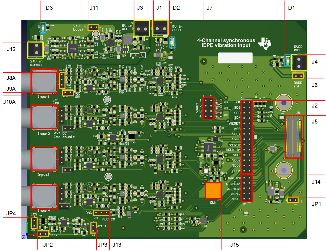
Figure 4-2 shows various connectors and jumpers used to interface with the design PCB.
 Figure 4-2 PCB Interface
| CONNECTOR | DESCRIPTION |
|---|---|
| J9A…J9D | Ch1 to Ch4 sensor input (BNC connector, with shield grounded) |
| J8A…J8D | Ch1 to Ch4 excitation
current source selector Short (3,2) top and middle, to use onboard current source (make sure it is powered) Connect external current source (2,1) middle and bottom, to use external current source Leave open to evaluate the channel without excitation current (no sensor is connected) |
| J10A…J10D | Ch1 to Ch4 coupling
selection Short: DC coupling, use for Ch4 in case of DC coupling, other channels for testing Open: AC coupling, default configuration |
| J5 | QHS connector connect to PHI, best practice is to power the board before connection |
| J2 | SPI signals header, use for debugging and probing, or to connect to another board (if no QHS) |
| J14 | DAC and SR signals header, use for driving (no QHS) or monitoring auxiliary signals |
| J7 | nRDY signal header, use for checking the synchronization between ADCs |
| J15 | SMA connector for Clk, based on the assembly can be used either as clock input (crystal is removed), or as a clock output |
| JP1 | Used for EEPROM programming if needed. Not used for the PHI board |
| J12 | External supply for excitation current, if used, make sure J11 is open, D3 indicates active supply |
| J11 | Short to use onboard booster supply for excitation current, make sure J12 is open |
| J3 | Input supply for onboard booster stage, valid input range is 1.8 V to 5.5 V, typically use 5.2 V |
| J1 | Input supply for onboard LDO generating 5 V, valid input range is 5.2 V to 6 V, use 5.2 V |
| J4 | External digital supply, recommended to use 2.5 V. When used make sure J6 is open and that the MCU or controller connected is 2.5-V compatible. |
| J6 | Short to use PHI digital supply (make sure 2.5 V, and J4 is open), open if external supply is to be used |
| J13 | DAC connection short (1,2, right) to use ADC CM (2.5 V) as input attenuator common-mode short (2,3, left) to use DAC as common-mode source for the attenuator use pin1 to monitor ADC CM, pin3 to monitor, use DAC output, pin2 to connect external source |
| JP3 | Control connection for variable current source, connect J13, pin3 to use the DAC |
| JP2 | Supply connection for the variable current source (note ground sign) |
| JP4 | Output connection for variable current source, connect to J8x(1,2) to use as channel ISOURCE |